Combination nonvolatile memory using unified technology with byte, page and block write and simultaneous read and write operations

a non-volatile memory, unified technology, applied in the field of semiconductor memory, can solve the problems of drastic system performance degradation, difficult use of flash memory to store both program code and data, and inconvenient us

Inactive Publication Date: 2005-06-30
CALLAHAN CELLULAR L L C
View PDF14 Cites 12 Cited by
  • Summary
  • Abstract
  • Description
  • Claims
  • Application Information

AI Technical Summary

Benefits of technology

[0020] It is an objective of the present invention to provide a non-volatile memory technology, cell structure, array architecture, and operations that allows using a single technology to manufacture both Flash memory array and EEPROM array in one chip.
[0032] In the present invention a unified technology is created from which an EEPROM memory cell has evolved that incorporates the non-volatile storage element of a Flash memory cell into the EEPROM cell. The EEPROM cell also contains a select transistor, which has been sized to allow the EEPROM to be compatible with the bit line pitch of the Flash memory cell. This is accomplished by reducing the size of the select transistor which is a result of using a higher than normal program voltage on the gate of the select transistor. Pre-charging the node connecting the nonvolatile storage element and the select transistor of the EEPROM cell, or providing a virtual-ground scheme of each byte, prevents a select transistor break down. The precharge voltage or virtual-ground source “bucks” the high bit line voltage connected to non-selected cells in a selected column so that the Vds of the select transistor can be made smaller than the Vds of floating-gate cell. Thus, a shorter channel length of the select transistor can be made smaller than or equal to the channel length of the floating-gate device as required in CHE program operation.

Problems solved by technology

Using an EEPROM to store both the program code and data is not very cost effective because of the large cell size of the EEPROM.
Using Flash memory to store both the program code and data is not easy because Flash memory lacks the byte-level data alterability as provided in an EEPROM.
As a result, a highly complex software technique is required which causes drastic system performance degradation, and sometimes may cause reliability problem.
The integration of a Flash and EEPROM memory in a single memory chip is highly desirable for reducing cost, device footprint, and power consumptions while providing superior performance; however, since the cell structure and process technology is different between Flash and EEPROM memories, combining these two memories into one chip requires very complex process flow, which is not cost effective.

Method used


Image

  • Combination nonvolatile memory using unified technology with byte, page and block write and simultaneous read and write operations
  • Combination nonvolatile memory using unified technology with byte, page and block write and simultaneous read and write operations
  • Combination nonvolatile memory using unified technology with byte, page and block write and simultaneous read and write operations

Examples


Embodiment Construction

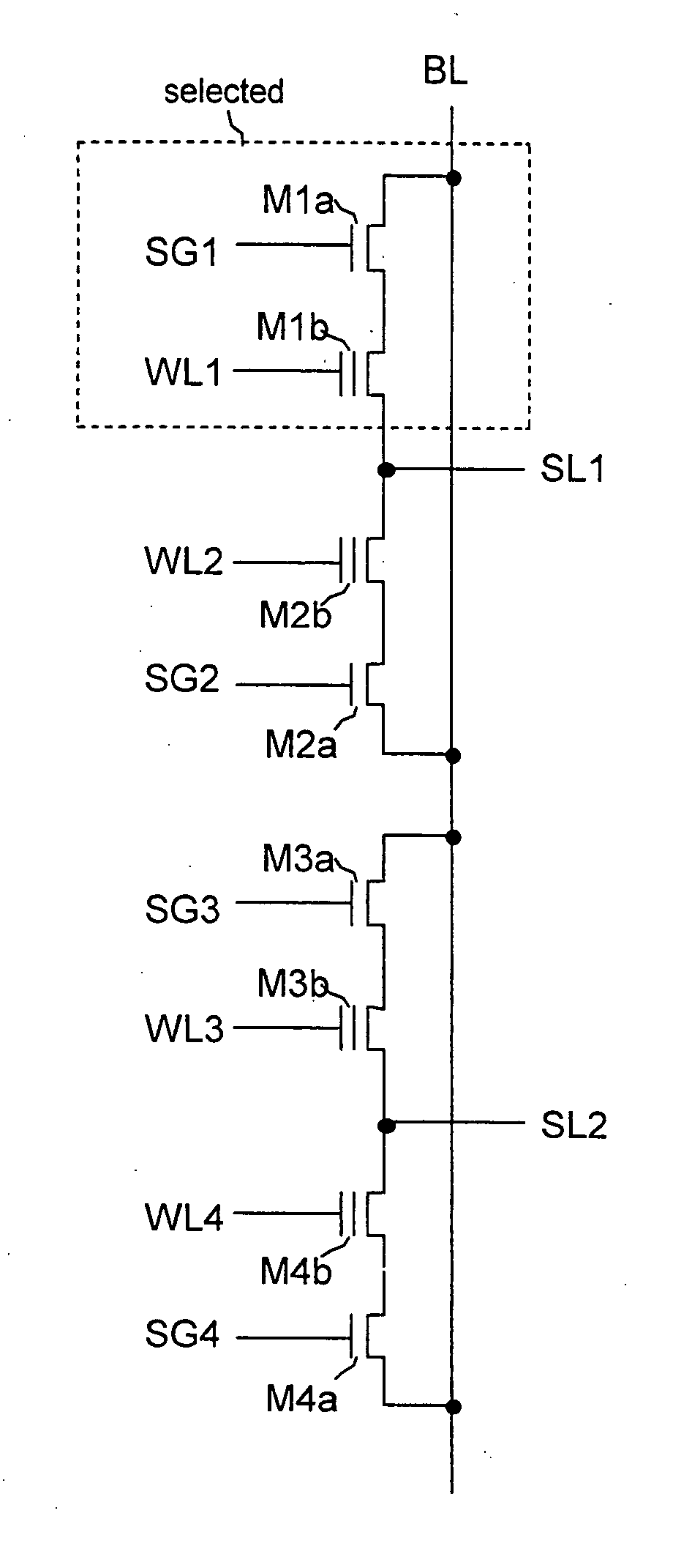
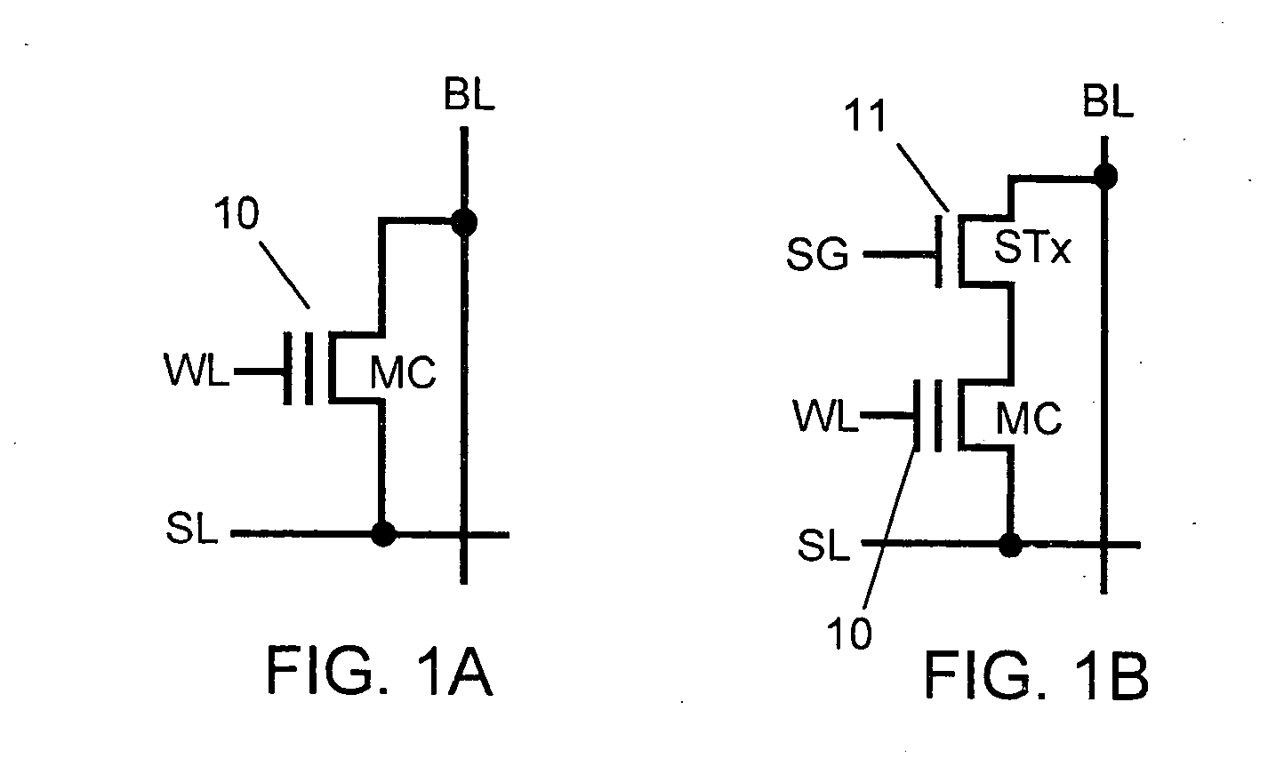
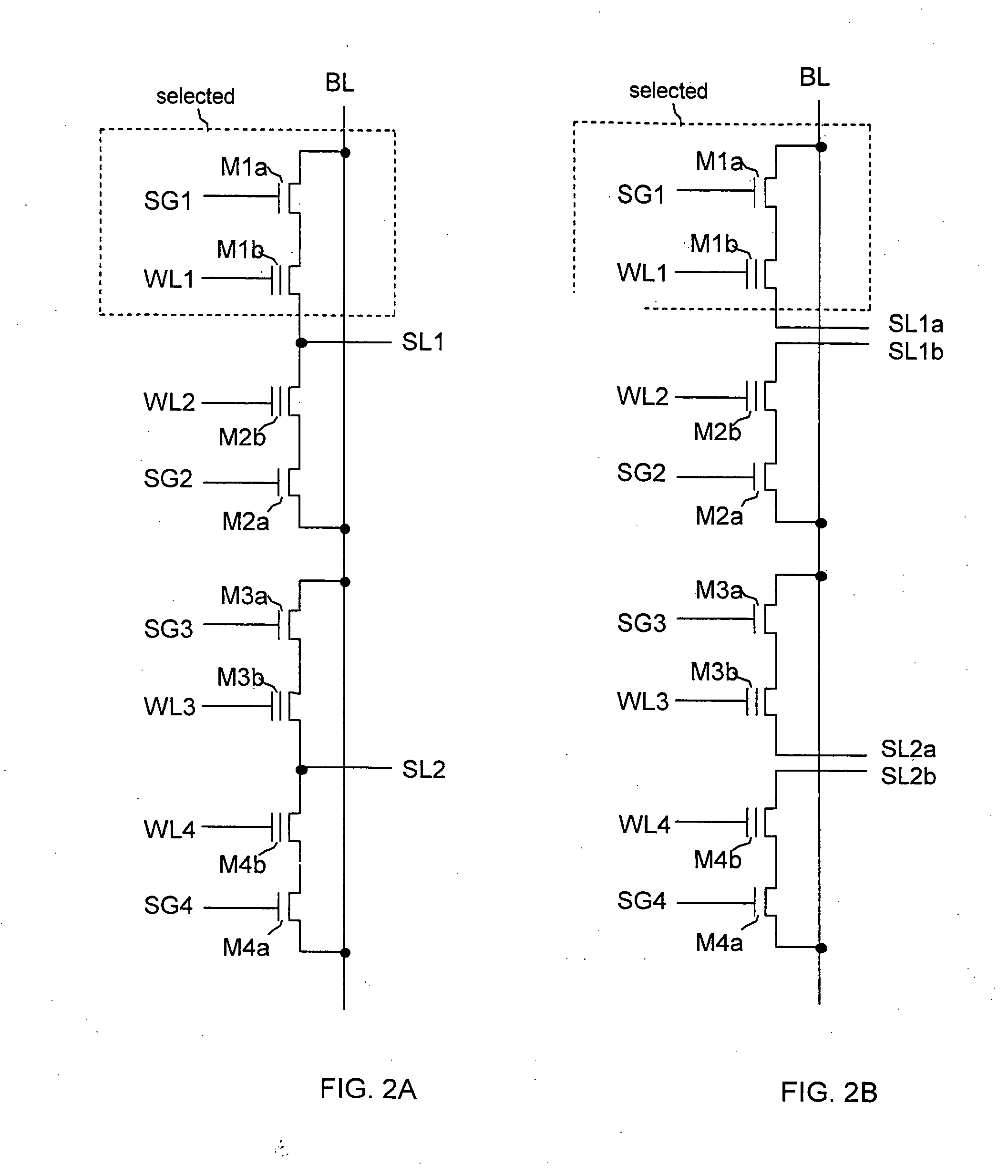
[0066] In FIG. 1A is shown a schematic diagram of the Flash memory cell MC of the present invention. The stacked gate transistor 10, which forms the memory cell, has a source diffusion connected to a source line SL and a drain diffusion connected to a bit line BL. The control gate of the stacked gate transistor is connected to a word line WL. The Flash cell of the present invention can be made smaller by reducing coupling ratio from Poly2 to floating-gate and by increasing word line voltage to maintain the same program gate voltages. The erase and program conditions of Flash are listed in Table 1 below.

TABLE 1VoltageBLWLSLBulkSchemeErase0−18 V00FN (Channel)Program+5 V+10 V00CHE

[0067] Shown in FIG. 1B is shown a schematic diagram of a two transistor EEPROM memory cell of the present invention. The Flash and EEPROM memory cells are fully described in Provisional Application Ser. No. 60 / 426,614 noted above which is herein included by reference. The stacked gate transistor 10 used in ...


PUM


Abstract

A combination EEPROM and Flash memory is described containing cells in which the stacked gate transistor of the Flash cell is used in conjunction with a select transistor to form an EEPROM cell. The select transistor is made sufficiently small so as to allow the EEPROM cells to accommodate the bit line pitch of the Flash cell, which facilitates combining the two memories into memory banks containing both cells. The EEPROM cells are erased by byte while the Flash cells erased by block. The small select transistor has a small channel length and width, which is compensated by increasing gate voltages on the select transistor and pre-charge bitline during CHE program operation.

Description

[0001] The present application is related to and claims benefit of priority of the filing date of U.S. Provisional Patent Application Ser. No. 60 / 394,202 filed on Jul. 5, 2002 and entitled “A Novel Monolithic Nonvolatile Memory Allowing Byte, Page and Block Write With No Disturb and Divided-Well in The Cell Array Using A Unified Cell Structure and Technology With A New Scheme of Decoder”, which is herein incorporated by reference. [0002] The present application is further related to and claims benefit of priority of the filing date of U.S. Provisional Patent Application Ser. No. 60 / 426,614 filed on Nov. 14, 2002, entitled “A Novel Monolithic, Combo Nonvolatile Memory Allowing Byte, Page And Block Write With No Disturb And Divided-Well In The Cell Array Using A Unified Cell Structure And Technology With A New Scheme Of Decoder And Layout”, which is herein incorporated by reference. [0003] The present application is further related to and claims benefit of priority of the filing date ...

Claims


Application Information

Patent Timeline
Patent Type & Authority Applications(United States)
IPC IPC(8): G11C16/04G11C16/14H01L21/8247H01L27/115
CPCG11C16/0408G11C16/0416G11C16/0433G11C16/14G11C16/16H01L27/11524G11C2216/18G11C2216/22H01L27/115H01L27/11521G11C16/3445H10B41/35H10B69/00H10B41/30G11C16/06
Inventor LEE, PETER W.HSU, FU-CHANGTSAO, HSING-YAMA, HAN-REI
Owner CALLAHAN CELLULAR L L C
Why Eureka
Try Eureka