Organic electroluminescence device and organic electroluminescence display

a technology of electroluminescence display and electroluminescence device, which is applied in the direction of discharge tube luminescnet display, natural mineral layered products, transportation and packaging, etc., can solve the problems of increased drive voltage, short circuit, and reduced light-emitting luminance, and achieves superior light-emitting efficiency and long service life.

Active Publication Date: 2005-06-30
FUJIFILM HLDG CORP +1
View PDF4 Cites 36 Cited by
  • Summary
  • Abstract
  • Description
  • Claims
  • Application Information

AI Technical Summary

Benefits of technology

[0019] The organic electroluminescence device as described above

Problems solved by technology

However, continuously driving the organic EL device over time results in a decreased light-emitting luminance and an increased drive voltage, eventually causing a short circuit.
It is considered that degradations of the organic EL device are due to crystallization over time of organic materials, the associated accumulation of space charges within the organic layer, and polarization due to applying the electric field in a certain direction, causing organic molecules to polarize the electrodes so as to change the electric characteristic of the device, or degradations due to oxidization of the electrodes, etc.
Moreover, when there is high power consumption, it is possible that the energy lost that changes to heat helps to degrade the organic material.
However, with this configuration, a decreased voltage at each organic layer and generated Joule heat due to the high-resistance characteristics of the organic layers lead to a decrease in the light-emitting efficiency and the service life of the organic EL device.
In this case, while it is possible that the conductivity can be enhanced to increase the amount of hole current and the amount of electron current, as the carriers are not enclosed sufficiently

Method used


Image

  • Organic electroluminescence device and organic electroluminescence display
  • Organic electroluminescence device and organic electroluminescence display
  • Organic electroluminescence device and organic electroluminescence display

Examples


first embodiment

A First Embodiment

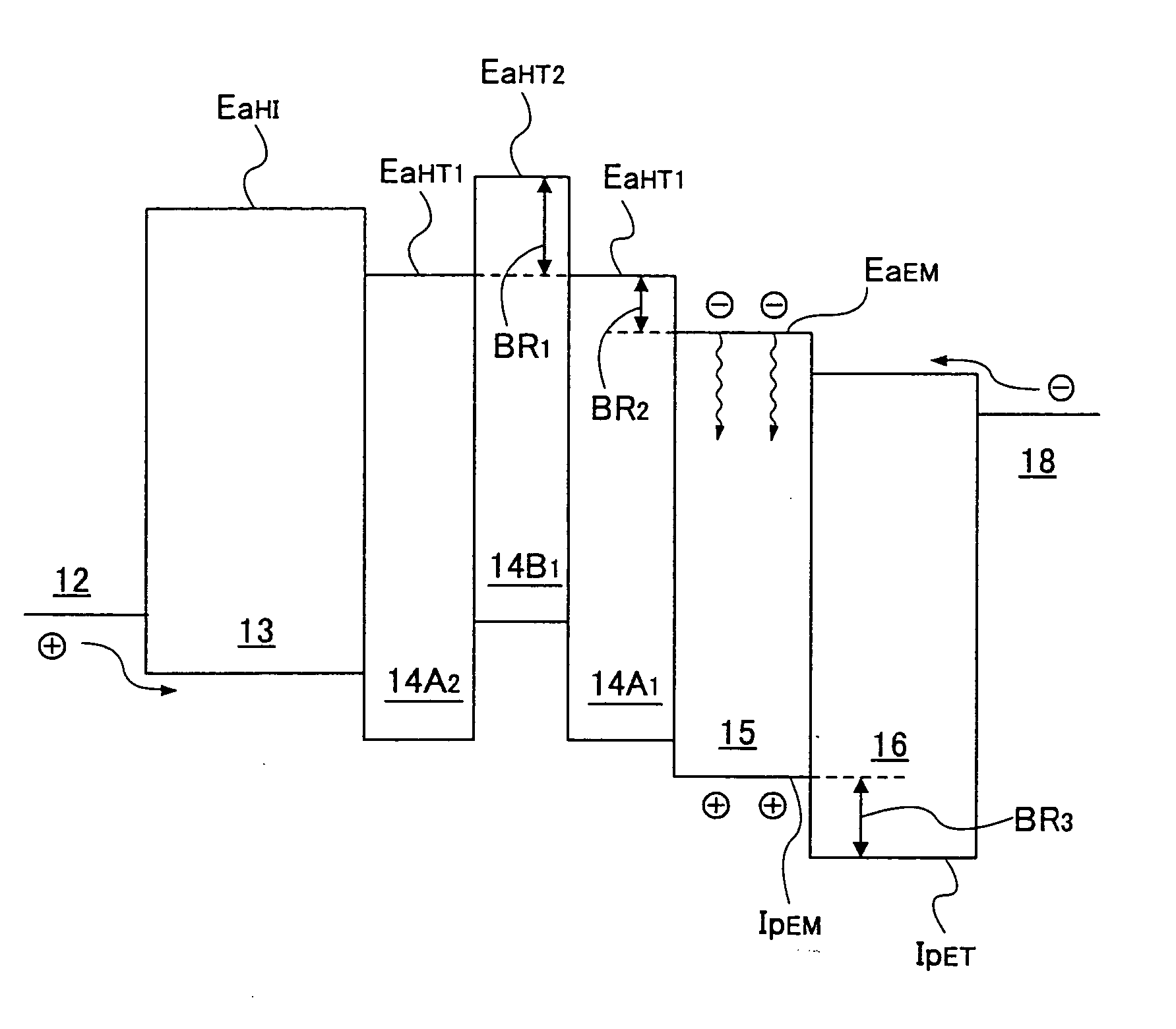
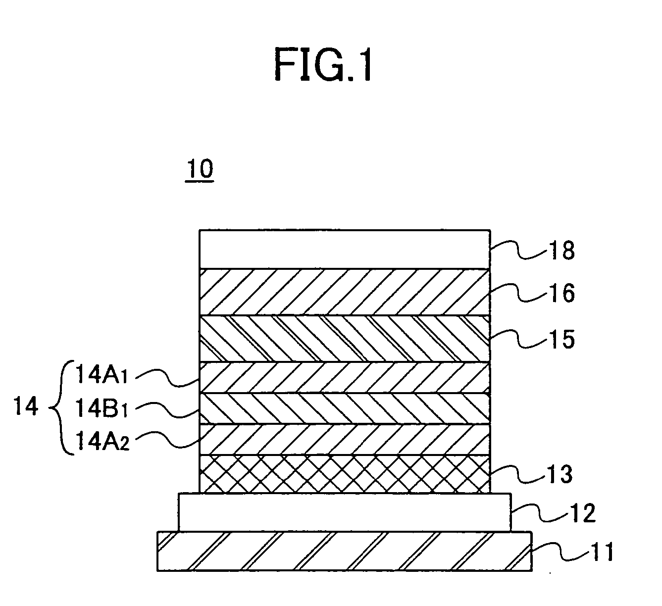
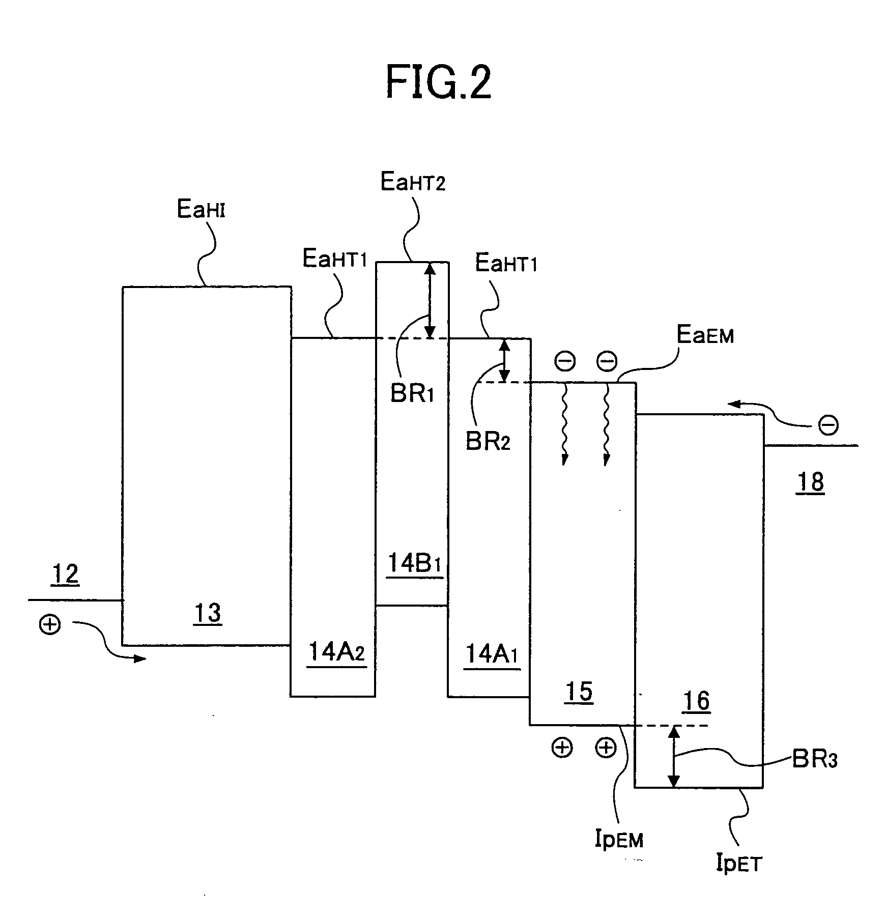
[0030]FIG. 1 is a cross-sectional view of an organic EL device according to the first embodiment of the present invention. FIG. 2 is an energy diagram of the organic EL device according to the first embodiment as illustrated in FIG. 1. In FIG. 2, Ea denotes the electron affinity and Ip denotes the ionizing potential. Referring to FIGS. 1 and 2, an organic EL device 10 is configured with a substrate 11, an anode 12, a hole-injecting layer 13, an electron-transporting suppressing stack 14, a light-emitting layer 15, an electron-transporting layer 16 and a cathode 18 that are sequentially formed on the substrate 11.

[0031] The organic EL device 10 of the present invention has the hole-injecting layer 13 composed of a hole-transporting material that is doped with acceptors. The hole-injecting layer 13 is, for example 2-TNATA(4,4′,4″-tris(2-naphthylphenylanimo)triphenylamine), a hole-transporting material doped with inorganic materials such as halogen metal compounds, h...

first example

A First Example

[0067] The organic EL device according to the present example is composed from an ITO anode, a hole-injecting layer, an electron-transporting suppressing stack consisting of three electron-transporting suppressing layers, a light-emitting layer, and a cathode that are formed on a transparent substrate.

[0068] A glass substrate with an ITO electrode is supersonically cleansed with water, acetone, and isopropylalcohol, and the surface of the anode is irradiated with UV light in the atmosphere for 20 minutes so as to perform a UV ozone process. Then using a vacuum-deposition apparatus with a vacuum of 1×10⁻⁶ torr and a substrate temperature at 20° C., 2-TNATA and F4-TCNQ as the hole injecting layers are simultaneously deposited at the respective deposition rate of 0.5 nm / s and 0.0005 nm / s and are each set to have the thickness of 120 nm. In other words, with 2-TNATA being 100 vol. %, the content of F4-TCNQ was set at 0.1 vol. %.

[0069] Then, the electron-transporting sup...

second embodiment

A Second Embodiment

[0075]FIG. 8 is an exploded perspective view of the organic EL display according to the second embodiment of the present invention. Referring to FIG. 8, an organic EL display 30 is configured with a glass substrate 31, and a cathode 32 formed on the glass substrate in a stripe shape, an anode 34 formed vertically opposing the cathode 31 in a stripe shape, and a stack 33, etc., formed between the cathode 32 and the anode 34. Moreover, the organic EL display 30 is configured with a drive circuit (not illustrated) for driving a voltage to be applied between the cathode and the anode, and an encapsulated container, etc., for preventing exposure to moisture.

[0076] In the organic EL display 30 a voltage is applied to the cathode 32 and the anode 34 of a desired region causing emitting light in the desired region. The feature of the organic EL display is that the organic EL device consisting of the anode 34, the stack 33 and the cathode 32 is composed from the organic E...


PUM

PropertyMeasurementUnit
Thicknessaaaaaaaaaa
Thicknessaaaaaaaaaa
Electron affinityaaaaaaaaaa

Abstract

An organic electroluminescence device is disclosed. The device includes an anode, a cathode formed above the anode, a light-emitting layer containing an organic light-emitting material that is formed between the anode and the cathode, a hole-injecting layer on the anode that includes a hole-transporting material and an acceptor, and an electron-transporting suppressing stack between the hole-injecting layer and the light-emitting layer. The electron-transporting suppressing stack consists of multiple carrier-transporting layers, and forms energy barriers relative to electrons flowing from the light-emitting layer to the hole-injecting layer.

Description

CROSS-REFERENCE TO RELATED APPLICATION [0001] This application is a U.S. continuation application filed under 35 USC 111(a) claiming benefit under 35 USC 120 and 365(c) of PCT application JP2003 / 004225, filed Apr. 2, 2003. The foregoing applications are hereby incorporated herein by reference.BACKGROUND OF THE INVENTION [0002] 1. Field of the Invention [0003] The present invention generally relates to a technology for a photoelectronic device and a flat-panel display using a photoelectronic device, and particularly relates to an organic electroluminescence device and an organic electroluminescence display. [0004] 2. Description of the Related Art [0005] In recent years, there has been a gradual shift in market needs from a conventional large and weighty CRT (a Braun tube) display to a thin and light-weight flat display. As for flat displays, LCD displays and plasma displays have been brought to commercial use as household television sets and PC monitors, etc. [0006] Recently and con...

Claims


Application Information

Patent Timeline
IPC IPC(8): H01L51/00H01L51/50H05B33/12H05B33/14H05B33/22
CPCH01L51/0051H01L51/0059H01L51/006H01L51/0077Y10T428/24942H01L51/5048H01L51/5088H01L51/5096H01L51/0081H10K85/611H10K85/631H10K85/633H10K85/30H10K85/324H10K50/14H10K50/17H10K50/18
Inventor ITAI, YUICHIRO
Owner FUJIFILM HLDG CORP
Why Eureka
Try Eureka