Method for fabricating nitride semiconductor, method for fabricating nitride semiconductor device, and nitride semiconductor device

a technology of nitride semiconductor and semiconductor, which is applied in the direction of semiconductor devices, semiconductor lasers, semiconductor lasers, etc., can solve the problems of conventional doping techniques that find it difficult to provide a steep impurity profile, insufficient superlattice structure of p-type cladding layer, and insufficient nitride semiconductor resistance. achieve the effect of low nitride resistance, steep p-type impurity profile, and increase the p-type impurity density

Inactive Publication Date: 2005-06-30
PANASONIC SEMICON SOLUTIONS CO LTD
View PDF9 Cites 19 Cited by
  • Summary
  • Abstract
  • Description
  • Claims
  • Application Information

AI Technical Summary

Benefits of technology

[0010] An object of the present invention is attaining low resistance of a nitride semiconductor by increasing the p-type impurity density of the nitride semiconductor without increasing the doping amount and also providing a steep p-type impurity profile.

Problems solved by technology

In the first prior art, the superlattice structure of the p-type cladding layer is yet insufficient in attaining low resistance.
In addition, the conventional doping techniques find difficulty in providing a steep impurity profile.

Method used


Image

  • Method for fabricating nitride semiconductor, method for fabricating nitride semiconductor device, and nitride semiconductor device
  • Method for fabricating nitride semiconductor, method for fabricating nitride semiconductor device, and nitride semiconductor device
  • Method for fabricating nitride semiconductor, method for fabricating nitride semiconductor device, and nitride semiconductor device

Examples


Embodiment Construction

[0042] Hereinafter, a preferred embodiment of the present invention will be described with reference to the accompanying drawings.

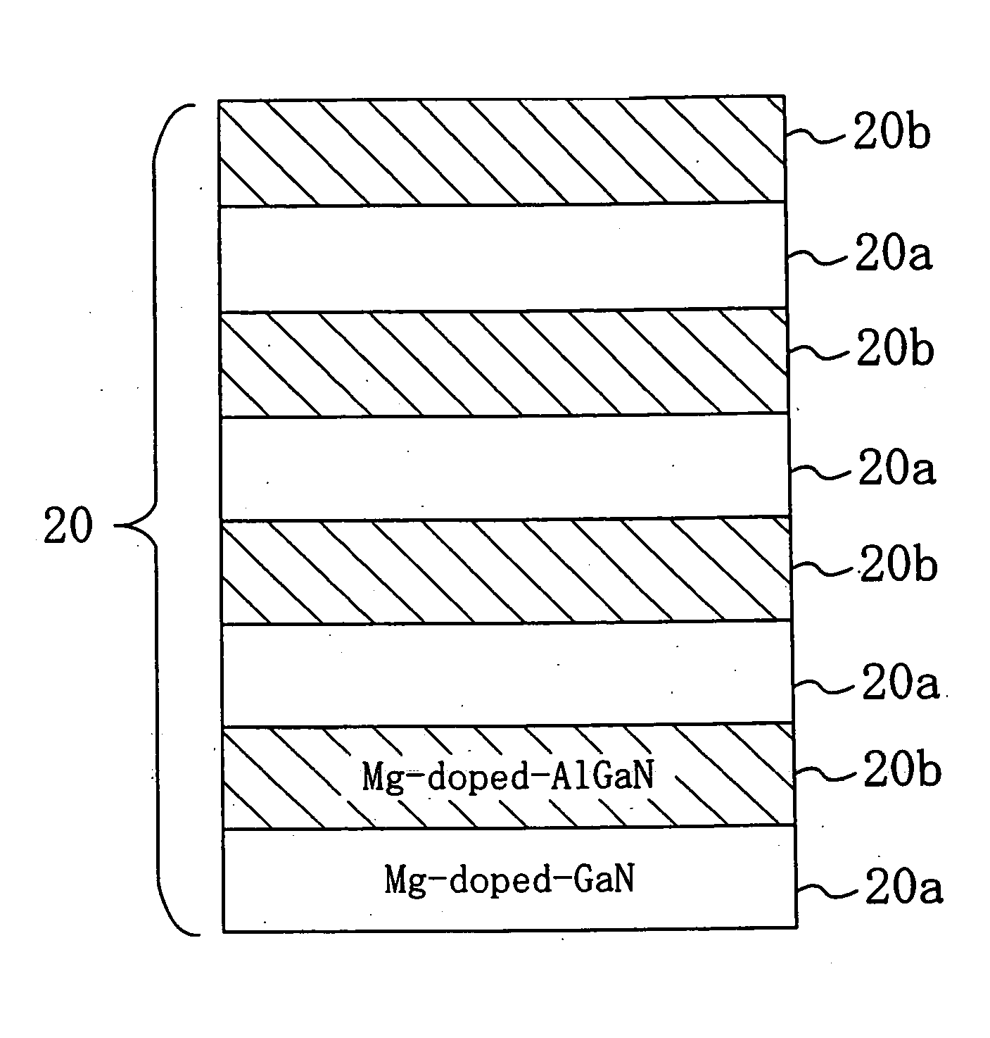
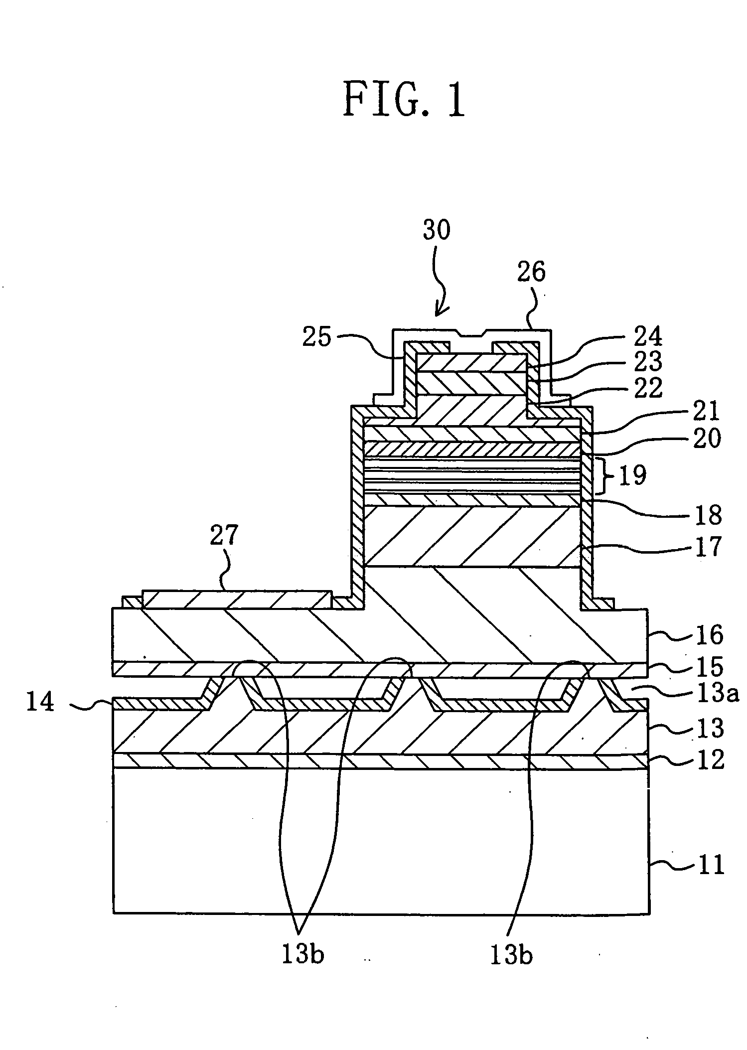
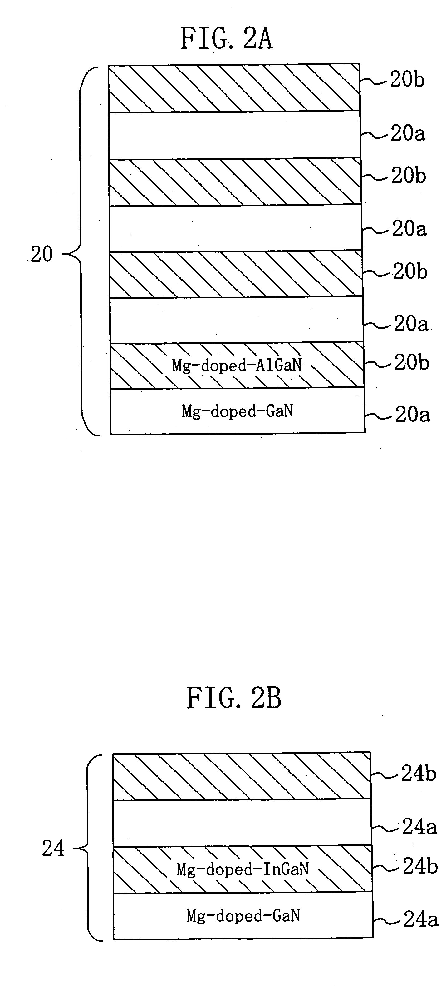
[0043]FIG. 1 shows a cross-sectional construction of a nitride semiconductor laser device in an embodiment of the present invention. Hereinafter, the construction of the semiconductor laser device will be described together with the fabrication process thereof. Metal-organic vapor phase epitaxy (MOVPE) is employed for crystal growth, and the growth pressure may be a decompressed pressure, the atmospheric pressure (1 atm), or a compressed pressure higher than the atmospheric pressure. Alternatively, the growth pressure may be changed to an appropriate pressure for each semiconductor layer. As a carrier gas for supplying a material gas to the substrate, at least an inert gas such as nitrogen or hydrogen is used.

[0044] Referring to FIG. 1, first, the growth temperature is set at about 500° C., and ammonia (NH3) as a group V source and trimethylgallium (TMG...


PUM

PropertyMeasurementUnit
thicknessaaaaaaaaaa
thicknessaaaaaaaaaa
thicknessaaaaaaaaaa

Abstract

The method for fabricating a nitride semiconductor of the present invention includes the steps of: (1) growing a first semiconductor layer made of a first group III nitride over a substrate by supplying a first group III source and a group V source containing nitrogen; and (2) growing a second semiconductor layer made of a second group III nitride on the first semiconductor layer by supplying a second group III source and a group V source containing nitrogen. At least one of the steps (1) and (2) includes the step of supplying a p-type dopant over the substrate, and an area near the interface between the first semiconductor layer and the second semiconductor layer is grown so that the density of the p-type dopant locally increases.

Description

BACKGROUND OF THE INVENTION [0001] The present invention relates to a method for fabricating a nitride semiconductor in which the density of a p-type dopant is positively increased, a method for fabricating a nitride semiconductor device, and a nitride semiconductor device fabricated by this method. [0002] Prior art techniques of doping a nitride semiconductor device with a p-type dopant, in particular, magnesium (Mg) will be described. [0003] In the first prior art (Japanese Journal of Applied Physics, 38, L1012, 1999), a superlattice (SL) layer having a cycle of 36 nm is disclosed for use as a p-type cladding layer paired with an n-type cladding layer to sandwich an active layer in the direction vertical to a substrate and confine light generated from the active layer. Each cycle of the superlattice layer is composed of an aluminum gallium nitride (Al0.15Ga0.85N) layer having a thickness of 24 nm and a gallium nitride (GaN) layer having a thickness of about 12 nm, for example. In ...

Claims


Application Information

Patent Timeline
Patent Type & Authority Applications(United States)
IPC IPC(8): H01S5/30H01L21/20H01L21/205H01L33/00H01L33/32H01S5/323H01S5/343
CPCB82Y20/00H01S2304/12H01L21/02458H01L21/02507H01L21/0254H01L21/02579H01L21/0262H01L21/0265H01L33/007H01L33/32H01S5/22H01S5/3063H01S5/3215H01S5/3216H01S5/34333H01S2304/04H01L21/0242H01S5/30
Inventor ISHIBASHI, AKIHIKOTSUJIMURA, AYUMUHASEGAWA, YOSHIAKIOTSUKA, NOBUYUKISUGAHARA, GAKUMIYANAGA, RYOKOSHIMAMOTO, TOSHITAKAHARAFUJI, KENJIBAN, YUZABUROOHNAKA, KIYOSHI
Owner PANASONIC SEMICON SOLUTIONS CO LTD
Why Eureka
Try Eureka