

Method of manufacturing semiconductor device, film-forming apparatus, and storage medium
a technology of film-forming apparatus and semiconductor devices, which is applied in the direction of semiconductor devices, electrical devices, basic electric elements, etc., can solve the problems of limited operation speed, flat band voltage (vfb, hafnium compound films), etc., and achieve the effect of high dielectric constan
- Summary
- Abstract
- Description
- Claims
- Application Information
AI Technical Summary
Benefits of technology
Problems solved by technology
Method used
Image


Examples
example 1
A. Example 1
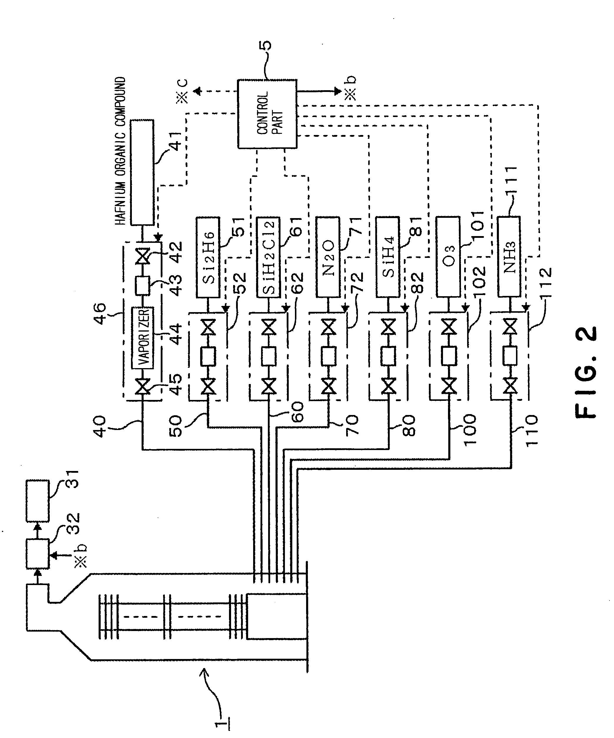
[0068] A hafnium silicate film as a gate insulating film was formed on a surface of a P-type silicon film on a wafer, by using a film-forming apparatus of the same kind as the above-described film-forming apparatus. Then, a CVD silicon oxide film as a barrier layer, and a polysilicon film as a gate electrode were formed in that order, by using the same film-forming apparatus. The thus formed layered body is referred to as Example 1. Process conditions for the respective films, and their film thicknesses were as follows:
[Process Conditions for Hafnium Silicate Film]
[0069] specified temperature: 200 to 300° C. [0070] specified pressure: 0.3 to 0.5 Torr [0071] specified flow rate of tetra-tertiary-butoxy hafnium: 0.1 to 0.3 sccm [0072] specified flow rate of disilane gas: 200 to 400 sccm [0073] film thickness: 25 Å
[Process Conditions for CVD Silicon Oxide Film][0074] specified temperature: 700 to 750° C. [0075] specified pressure: 0.4 Torr [0076] specified flow rate of d...
example 2
B. Example 2
[0083] A hafnium silicate film, a CVD silicon oxide film, and a polysilicon films were formed on a silicon film in the same manner as that of Example 1. Then, the hafnium silicate film was annealed by an ammonia (NH3) gas in a heating atmosphere of 600 to 800° C. The thus formed layered body is refereed to as Example 2.
example 3
E. Example 3
[0086] A hafnium silicate film as a gate insulating film was formed on a surface of an N-type silicon film on a wafer. Then, a silicon nitride film as a barrier layer, and a polysilicon film as a gate electrode were formed in that order, by means of the same film-forming apparatus. The thus formed layered body is referred to as Example 3. Process conditions for the hafnium silicate film and the polysilicon film were the same as those of Example 1. Process conditions for the silicon nitride layer were as follows.
[Process Conditions for Silicon Nitride Film]
[0087] specified temperature: 600 to 650° C. [0088] specified pressure: 0.15 Torr [0089] specified flow rate of dichlorosilane gas: 20 to 40 sccm [0090] specified flow rate of ammonia gas: 100 to 150 sccm [0091] film thickness: 3 to 10 Å
PUM
 Abstract
Description
Claims
Application Information