Optical article

a multi-aperture operation and optical technology, applied in the field of optical articles with optical multi-aperture operation, can solve the problems of reducing the conductivity and reflectivity affecting the radiation transmission efficiency of the buried layer, so as to reduce the alteration of the index of refraction of radiation transmission, improve radiation transmission, and eliminate or reduce the effect of reducing the alteration of the index of refraction

Inactive Publication Date: 2005-07-07
ROHM & HAAS ELECTRONICS MATERIALS LLC
View PDF28 Cites 39 Cited by
  • Summary
  • Abstract
  • Description
  • Claims
  • Application Information

AI Technical Summary

Benefits of technology

[0019] Selective passivation protects the electrically conductive metal and metal alloy layers from the harsh conditions when applying the material to encase the metal and metal alloys in the article. Additionally, selective passivation of the electrically conductive pattern eliminates or at least reduces alteration of the index of refraction of radiation transmission. Accordingly, the optical articles have improved radiation transmission over the radiation transmission of many conventional articles with passivated electrically conductive regions.
[0020] Selective passivation of the electrically conductive patterns also permits direct bonding of the material which encases the electrically conductive and selectively passivated patterns of the article. Since such materials are the same, a stronger interface bond is formed in contrast to articles having interface bonds between different materials. Accordingly, the probability of a separation of parts of the article at an interface is reduced, thus improving the reliability of the optical articles over many conventional articles.

Problems solved by technology

When the optical article is fabricated by providing a chemical vapor deposited material over a reflective or conductive surface, the high temperatures and the chemically corrosive environment often degrade the surface morphology of the highly reflective or conductive materials.
Further, when layers of the highly reflective metals such as gold or silver are used, the high temperatures and corrosive environment of the CVD process causes the layers to agglomerate.
However, during CVD, small islands of the material are formed leaving behind holes previously occupied by the material.
This degradation in the surface morphology leads to reduced conductivity and reflectivity of the buried layers.
Accordingly, buried layers containing highly reflective and conductive materials are not readily found within optical articles fabricated from chemically vapor deposited materials.
A disadvantage of the optical elements disclosed in the patent is that the passivating layers completely encompass the intermediate region with the electrically conductive refractory metals.
The change in the index of refraction of the radiation compromises the accuracy and over all performance of the optical elements.
Radiation is reflected at the refractive index change boundary, thus reducing the overall transmission of the optic.
In addition, radiation is bent as it passes through the passivation layer, due to the different refractive index, causing image distortion.
Another problem associated with the intermediate region of the optical elements is the bond interface between the passivating layers and both the base and overcoat layers.
This weak bond may result in the separation of the passivating layers from both the overcoat and base layers compromising operation of the optical elements or completely disrupting their operation.

Method used


Image

  • Optical article
  • Optical article
  • Optical article

Examples


example 1

Multi-aperture Zinc Sulfide Articles with Titanium-Tungsten (Ti—W) Conductive Layer

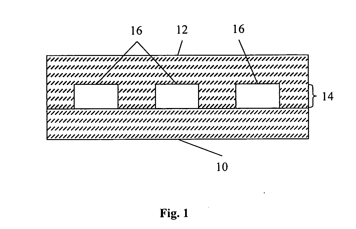
[0089] Zinc sulfide was produced by the reaction of elemental zinc with hydrogen sulfide at a temperature of 675° C. and a furnace pressure of 35 torr. The furnace was heated resistively using graphite heating elements. A graphite retort was mounted at the bottom of the furnace containing zinc. The retort was heated to a temperature of 700° C. to generate zinc vapor pressures of 5 torr. Zinc vapors were carried to the deposition area using argon as a carrier gas. Hydrogen sulfide at 3 torr was mixed with the argon at 28 torr and the mixture was introduced into the deposition area through a central injector. The hydrogen sulfide and zinc flow rates in the reactor provided a molar ratio of hydrogen sulfide to zinc sulfide during the reaction of 0.6 to 1. Zinc sulfide was deposited on the four inside walls of an open rectangular box. The average deposition rate of zinc sulfide was 1 micron / minute. The i...

example 2

Multi-Aperture Zinc Sulfide Articles with Tantalum (Ta) Conductive Layer

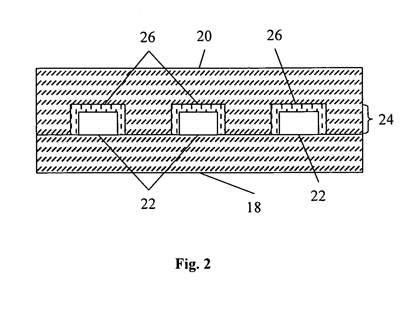
[0094] Water clear zinc sulfide substrates are prepared according to the method of Example 1 including the hipping process. A photoresist pattern is applied according to Example 1. Tantulum metal is deposited in the channels by sputtering using a conventional method such that the tantalum layer has a thickness of 20,000 Å. The photoresist remaining on the water clear zinc sulfide substrates is stripped using acetone. The photoresist with any deposited materials is lifted off the water clear zinc sulfide bases.

[0095] A zinc sulfide top coat is deposited on each zinc sulfide substrate base with the tantalum conductive grid using a CVD method as described in Example 1. After deposition of the zinc sulfide top layer, the articles are machined, lapped and polished to a scratch / dig ratio of 80 / 50. No anti-reflection coating is applied to any of the articles. The zinc sulfide articles are measured for transmission an...

example 3

Multi-Aperture Zinc Sulfide Articles with Molybdenum (Mo) Conductive Layer

[0096] Water clear zinc sulfide substrates are prepared according to the method of Example 1. A photoresist pattern is applied according to Example 1.

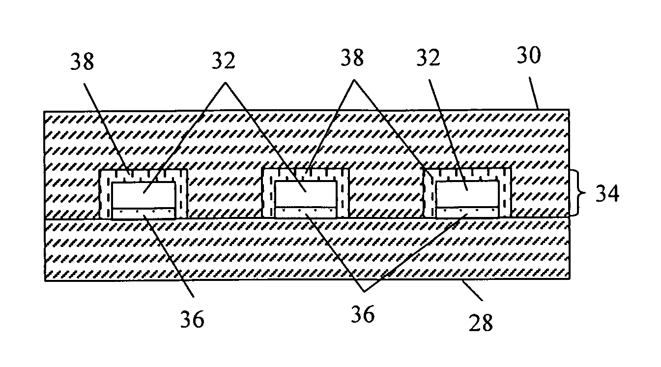
[0097] Titanium metal having a thickness of 300 Å is deposited in the channels using a conventional sputtering deposition method. After the deposition of the titanium layer, a layer of titanium dioxide having a thickness of 500 Å is deposited on the titanium layer by a conventional e-beam physical vapor deposition method. Molybdenum having a thickness of 10,000 Å is deposited on the titanium dioxide layer by a conventional sputtering deposition technique. The photoresist remaining on the water clear zinc sulfide is stripped using acetone. The photoresist with any deposited materials is lifted off the water clear zinc sulfide bases. In order to passivate and protect the exposed Ti / TiO2 / Mo metal during the subsequent overcoat deposition of zinc sulfide, the artic...


PUM


Abstract

An optical article and method of making the same are provided. The optical article has optical multi-aperture operation. The optical article has one or more electrically conductive and selectively passivated patterns.

Description

[0001] The present application is a non-provisional application of U.S. provisional application Ser. No. 60 / 517,932, filed Nov. 6, 2003.BACKGROUND OF THE INVENTION [0002] The present invention is directed to an optical article with optical multi-aperture operation. More specifically, the present invention is directed to an optical article with optical multi-aperture operation having electrically conductive and selectively passivated patterns. [0003] Optical articles, which may transmit various forms of radiation, are in demand in various industries. Examples of industries where optical articles are used include the electronics, nautical and aeronautics industries. Optical articles include windows, domes, and lenses, which are used to protect electronic devices on terrestrial, nautical and aeronautical vessels from undesired electromagnetic interference as well as other forms of radiation that may interfere with the optimum performance of such devices. [0004] A process known as chemi...

Claims


Application Information

Patent Timeline
Patent Type & Authority Applications(United States)
IPC IPC(8): G02B1/10G02B5/00H05B3/86
CPCG02B1/10H05B2203/013G02B5/00
Inventor GOELA, JITENDRA S.PICKERING, MICHAEL A.BROWN, NEIL D.CHIRAFISI, ANGELOLEFEBVRE, MARKTRIBA, JAMIE L.
Owner ROHM & HAAS ELECTRONICS MATERIALS LLC
Why Eureka
Try Eureka