Novel nitride barrier layer to prevent metal (Cu) leakage issue in a dual damascene structure

Inactive Publication Date: 2005-07-14
TAIWAN SEMICON MFG CO LTD
View PDF14 Cites 29 Cited by
  • Summary
  • Abstract
  • Description
  • Claims
  • Application Information

AI Technical Summary

Benefits of technology

[0015] An objective of the present invention is to provide a composite barrier layer that has g

Problems solved by technology

Unfortunately, the fabrication of microelectronic devices with copper has some drawbacks.
Since oxides do not block copper ions and may easily react with copper to produce undesirable copper oxides that reduce the conductivity of the copper layer, a barrier layer is frequently comprised of nitrogen in the form of a metal nitride or silicon nitride.
A problem occurs during a popular method of depositing a silicon nitride barrier layer on the first copper layer by a plasma enhanced chemical vapor deposition (PECVD) process.
The thin CuSiX layer on the first copper layer is responsible for causing a metal leakage problem in the resulting device.
Inadequate adhesion may lead to peeling of the silicon nitride barrier layer which has an adverse eff

Method used


Image

  • Novel nitride barrier layer to prevent metal (Cu) leakage issue in a dual damascene structure
  • Novel nitride barrier layer to prevent metal (Cu) leakage issue in a dual damascene structure
  • Novel nitride barrier layer to prevent metal (Cu) leakage issue in a dual damascene structure

Examples


Example

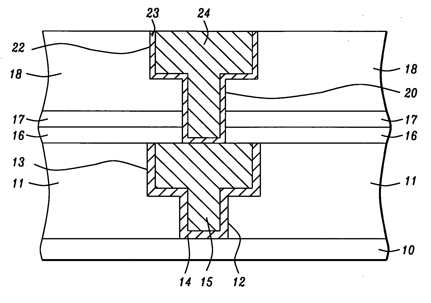
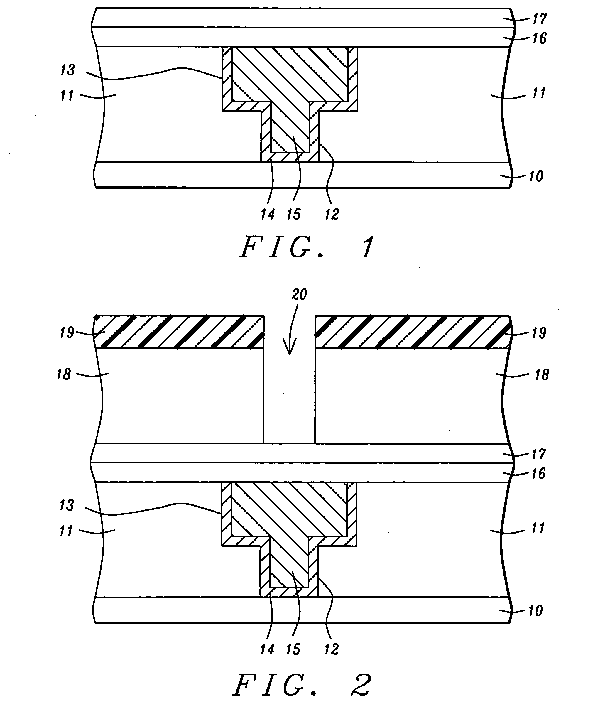
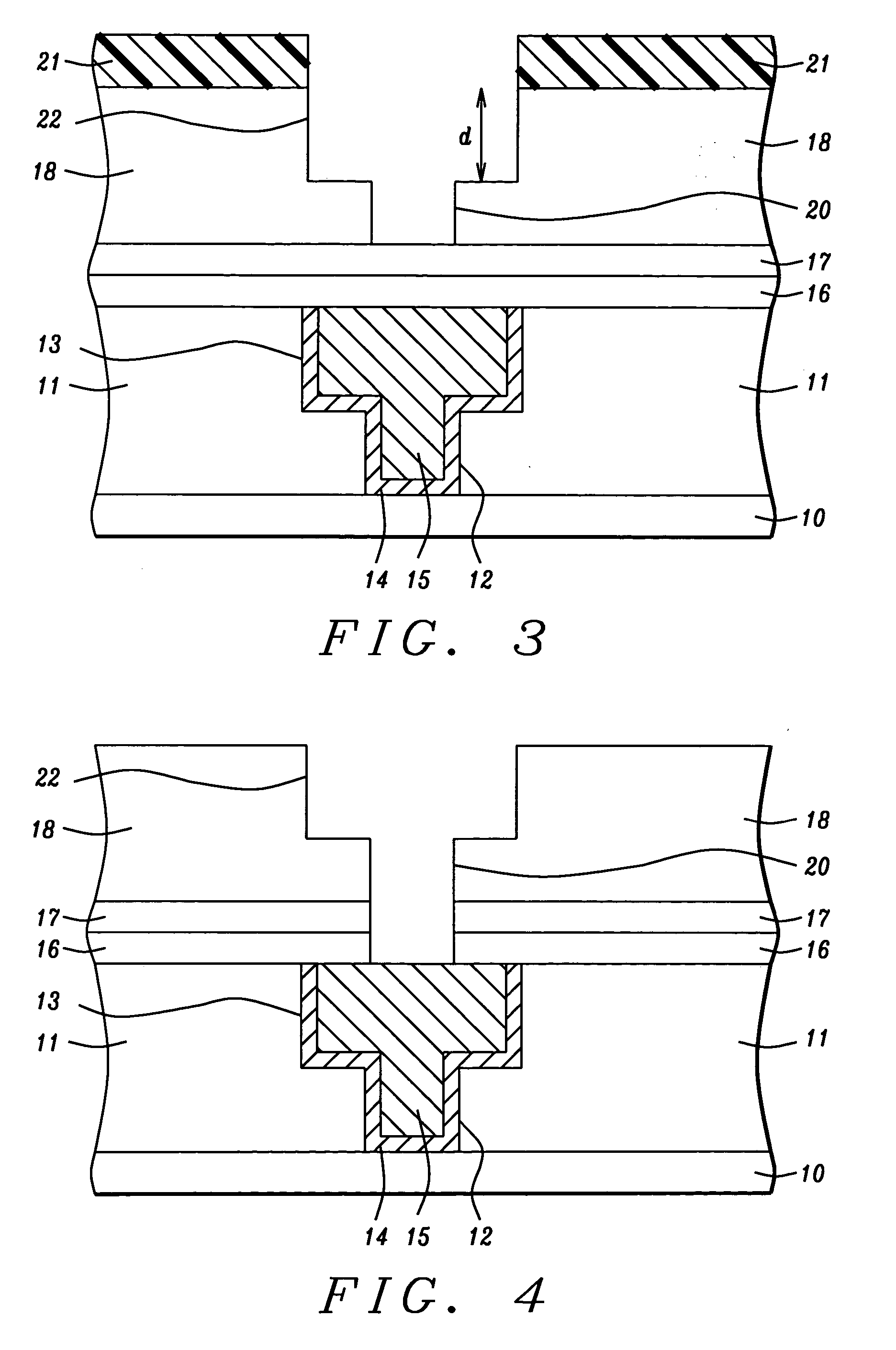
[0028] The present invention is particularly useful in forming a microelectronics device in which a conductive layer is formed on a copper layer and the device includes a composite barrier layer between the copper layer and an interlevel dielectric (ILD) layer. The composite barrier layer also serves as an etch stop layer in a damascene process flow. Although a dual damascene process is illustrated in the drawings, the composite barrier layer of the present invention may be formed on a substrate in a single damascene process or in other applications where a barrier layer also functions as an etch stop layer. It is understood that the drawings are provided by way of example and are not intended to limit the scope of the invention. In addition, the various elements within the drawings are not necessarily drawn to scale and the relative sizes thereof may be different than in an actual microelectronics device.

[0029] The invention will be described first in terms of a method of forming ...


PUM


Abstract

A method for forming a composite barrier layer that also functions as an etch stop in a damascene process is disclosed. A SiC layer is deposited on a substrate in a CVD process chamber followed by deposition of a silicon nitride layer to complete the composite barrier layer. The SiC layer exhibits excellent adhesion to a copper layer in the substrate and is formed by a method that avoids reactive Si+4 species and thereby prevents CuSiX formation. The silicon nitride layer thickness is sufficient to provide superior barrier capability to metal ions but is kept as thin as possible to minimize the dielectric constant of the composite barrier layer. The composite barrier layer provides excellent resistance to copper oxidation during oxygen ashing steps and enables a copper layer to be fabricated with a lower leakage current than when a conventional silicon nitride barrier layer is employed.

Description

FIELD OF THE INVENTION [0001] The invention relates to the field of fabricating integrated circuits and other electronic devices and in particular to an improved method of forming a composite barrier layer that reduces leakage from a copper interconnect fabricated by a damascene process. BACKGROUND OF THE INVENTION [0002] The manufacture of an integrated circuit in a microelectronics device involves the formation of several patterned metal layers that are successively overlaid upon one another to provide horizontal and vertical electrical pathways. These pathways are often referred to as metal wiring and are typically in the form of horizontal lines as well as vias and contacts which form vertical connections between the metal lines. An intermetal dielectric (IMD) layer is generally formed between the metal wiring to insulate the electrical pathways and prevent crosstalk that degrades device performance by slowing circuit speed. [0003] With the constant demand for microelectronics d...

Claims


Application Information

Patent Timeline
IPC IPC(8): H01L21/4763H01L21/768H01L23/52
CPCH01L21/76807H01L21/76832H01L21/76826
Inventor CHENG, YI-LUNGWANG, YING-LUNG
Owner TAIWAN SEMICON MFG CO LTD
Why Eureka
Try Eureka