Method and apparatus for providing optoelectronic communication with an electronic device

a technology of optoelectronic communication and electronic devices, applied in the direction of optical elements, instruments, semiconductor/solid-state device details, etc., can solve the problems of signal loss and distortion in the electrical transport media, the inability to scale to the bandwidth/distance requirements of next-generation servers, and the use of copper interconnect technology as the interconnect medium

Inactive Publication Date: 2005-07-21
IBM CORP
View PDF15 Cites 46 Cited by
  • Summary
  • Abstract
  • Description
  • Claims
  • Application Information

AI Technical Summary

Problems solved by technology

To connect between multiple MCMs, copper interconnect technology has been used as the interconnect medium, but is limited in its ability to scale to the bandwidth / distance requirements of next generation servers.
These limitations are primarily associated with the signal loss and distortion in the electrical transport media, such as printed circuit boards and connectors for example, and bandwidth reduction due to skin effect at high data transmission rates.
There have been a number of proposed inventions for integrating optical transceivers into modules, but they have had varying drawbacks for practicality and utility in computing systems.
This drawback will limit (a) the maximum possible number of signal channels, due to the 1-dimensional nature of the electrical signal path array from CMOS to O / E devices, and (b) the bandwidth per signal path.
In addition, the non-planarity of this package will make the assembly somewhat difficult.
Moreover, since the n×n laser arrays typically emit light perpendicular to the surface of the device, the optical interconnection and heat removal approaches are many times at odds with each other for these devices.
Since each of these functions requires a full 2-dimensional surface, to operate most effectively, an ideal packaging technology would have 3 surfaces, which is difficult, for planar devices.

Method used


Image

  • Method and apparatus for providing optoelectronic communication with an electronic device
  • Method and apparatus for providing optoelectronic communication with an electronic device
  • Method and apparatus for providing optoelectronic communication with an electronic device

Examples


Embodiment Construction

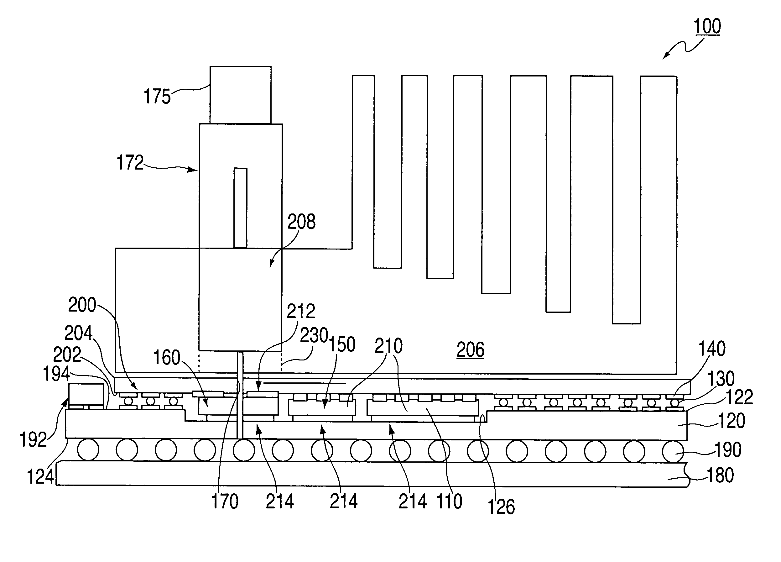
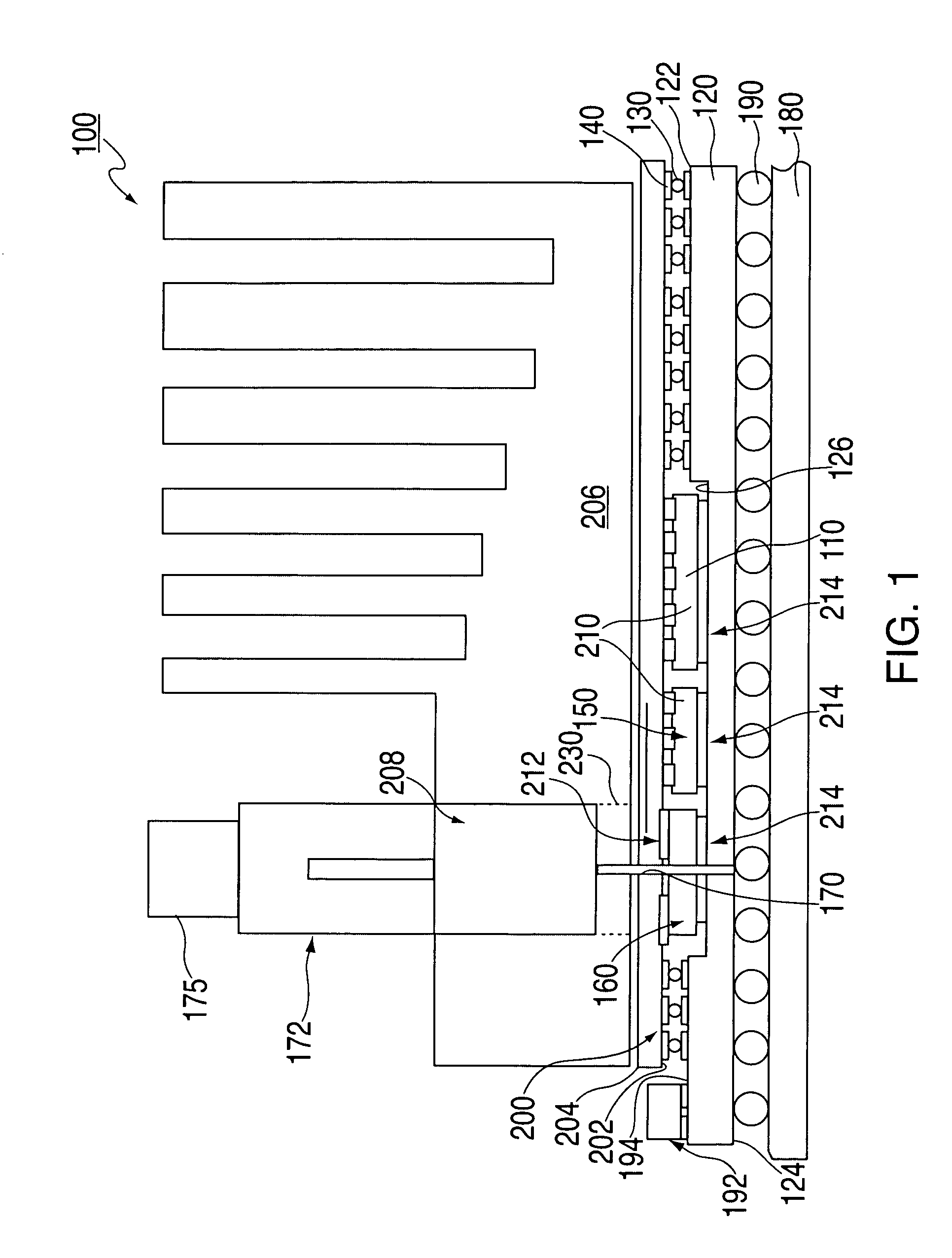
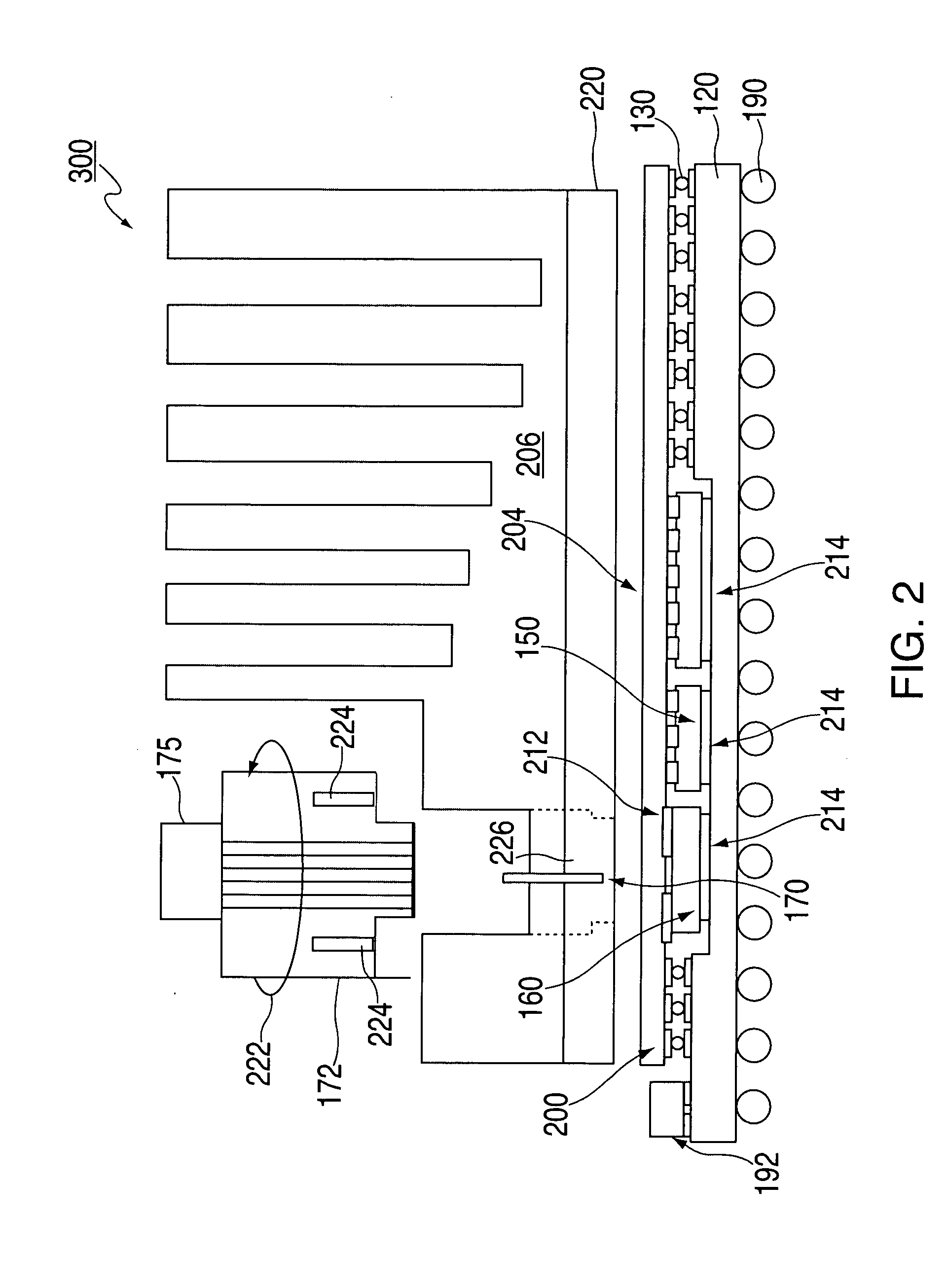
[0021] An embodiment of the present invention provides an optoelectronic assembly for a computer system having a signal communication path between an electronic computer or signal processing chip and an optoelectronic transducer that bypasses a printed circuit board, thereby providing high speed communication from the electronic chip to other components in the computer system. Another embodiment provides a high density optical signal path by using multiple optoelectronic transducers, alternatively referred to as a high density optical transceiver (HDOT). While embodiments described herein depict the interconnection of a processor complex within a Multi-Chip Module (MCM) to other processor complexes having an exemplary optoelectronic signal path, it will be appreciated that the disclosed invention is also applicable to the interconnection of other electronic devices housed in MCMs or SCMs (Single Chip Module), or other types of first level packaging. For example, embodiments of the i...


PUM

PropertyMeasurementUnit
lengthaaaaaaaaaa
transmission distancesaaaaaaaaaa
optoelectronicaaaaaaaaaa

Abstract

An optoelectronic assembly for an electronic system includes a transparent substrate having a first surface and an opposite second surface, the transparent substrate being thermally conductive and being metallized on the surface. A support electronic chip set is configured for at least one of providing multiplexing, demultiplexing, coding, decoding and optoelectronic transducer driving and receive functions and is bonded to the second surface of the transparent substrate. A first substrate having a first surface and an opposite second surface, is in communication with the transparent substrate via the metallized second surface and support chip set therebetween. A second substrate is in communication with the second surface of the first substrate and is configured for mounting at least one of data processing, data switching and data storage chips. An optoelectronic transducer is in signal communication with the support electronic chip set; and an optical signaling medium defined with one end having an optical fiber array aligned with the optoelectronic transducer is substantially normal to the first surface of the transparent substrate, wherein an electrical signal from the support electronic chip set is communicated to the optoelectronic transducer via the metallized second surface of the transparent substrate, and wherein the support electronic chip set and the optoelectronic transducer share a common thermal path for cooling.

Description

BACKGROUND OF THE INVENTION [0001] The present disclosure relates generally to optoelectronic communication with an electronic device, and particularly to the interconnection and attachment arrangement for providing optoelectronic communication between an electronic chip on a first level package and a high density optical transceiver. [0002] Typically, optoelectronic transceivers are mounted on a second level package, such as a printed circuit board, and are provided with their own heat sink and a means of being electrically interconnected with a printed circuit board, such as via a socket or a solder Ball Grid Array (BGA). The typical pitch of the electrical connections in a BGA is approximately 1.27 mm, although some products use finer pitches such as 1.0 or 0.8 mm. The size of an optoelectronic transceiver is largely determined by the area required by the heat sink and / or the area required for electrical connections between the optoelectronic transceiver and the second level pack...

Claims


Application Information

Patent Timeline
Patent Type & Authority Applications(United States)
IPC IPC(8): H01L31/0232
CPCG02B6/4212G02B6/4214G02B6/4292G02B6/4246G02B6/4249G02B6/4231G02B6/4269H01L2224/16225H01L2224/73253
Inventor BENNER, ALAN F.LIN, HOW TZUPOMPEO, FRANK L.SHINDE, SUBHASH L.
Owner IBM CORP
Why Eureka
Try Eureka