Optical waveguide evanescent ribbon coupler

a technology of optical waveguides and ribbon couplers, applied in the direction of optical waveguide light guides, instruments, optics, etc., can solve the problems of large distances required to interconnect devices and circuits on a common substrate, large delay, and large component size drop, so as to achieve high reliability, reduce production costs, and cost

Inactive Publication Date: 2006-11-28
SEC OF THE ARMY
View PDF3 Cites 43 Cited by
  • Summary
  • Abstract
  • Description
  • Claims
  • Application Information

AI Technical Summary

Benefits of technology

[0014]It is another object of the present invention to provide an optical coupler system that does not result in coupling power loss on the backplane waveguide when a card is not...

Problems solved by technology

Ongoing research and development efforts in very large scale integrated (VLSI) circuits have led to a dramatic decrease in component size and an increase in overall chip size.
One major limitation of packaged chips which use electrical interconnects is the relatively long distances required to interconnect devices and circuits on a common substrate or to connect chip packages on different circuit boards.
Ohmic power losses, long delay times escessive wafer space, and complex patterning techniques, are some of the other limitations associated with electrical interconnects.
Operating speed, for example, can be limited by external electromagnetic interference (EMI) from connecting lines, which can keep speeds to less than a few hundred MHz for compact systems.
This greatly limits its ability for fast computing and image data processing for both military and commercial applications.
However, there is no significant improvement on the computer motherboard because the existing interconnect still relies on electrical means that limit its improvement potential as mentioned above.
A comparison between optical and electrical interconnects, based on power and speed cons...

Method used


Image

  • Optical waveguide evanescent ribbon coupler
  • Optical waveguide evanescent ribbon coupler
  • Optical waveguide evanescent ribbon coupler

Examples


Embodiment Construction

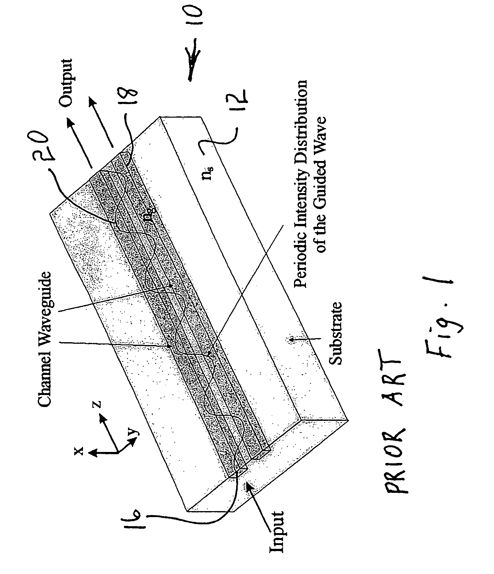
[0024]FIG. 1 shows a conventional prior art waveguide directional coupler structure 10. In this conventional configuration, a substrate 12 has mounted therein an input channel 16 and an adjacent output channel 18. The directional coupling results in the spatial periodic modulation of light intensity as shown by sinusoidal curve 20. Assume that the input light is in channel waveguide 16 at the point z=0 (see FIG. 1), the light intensities of the propagating mode in the two channel waveguides can be evaluated by the coupled mode theory and are given as follows

I1(z)=I0 COS2(κz),

I2(z)=I0 sin2(κz),  (1)

where I0=E02. κ is the coupling coefficient between the modes in the two waveguides 16 and 18 which depends strongly on the shape of the mode tails in the channel waveguides and the channel separation. κ can be determined by

[0025]κ=2⁢h2⁢p⁢⁢ⅇ-psβ⁡(w+2p)⁢(p2+h2),(2)

where

[0026] p2=⁢β2-ns2⁢k02,h2=⁢ng2⁢k02-β2,tan⁡(hw)=⁢2⁢p⁢⁢hh2-p2.(3)

Here, k0=ω / c. w is the channel width, s is the channel separa...


PUM


Abstract

An evanescent optically coupled electronic device including: a backplane wave guide or mother board including a set of parallel carriers that define a first plurality of parallel channels and include a first array of optical fibers having exposed cores in the first plurality of parallel channels; at least one electronic card or daughter board including a high speed optical waveguide bus; a flexible fiber ribbon or film including waveguides made up of individual optical fibers of locally increased refractive index joined by a web of suitable material forming the high speed optical waveguide bus and optically connecting the backplane waveguide and the at least one electronic card with no 90° angle turns; and a mechanism for retaining the first array of optical fibers having exposed cores in abutting and facing evanescent optical contact with the individual optical fibers in the flexible fiber or ribbon.

Description

[0001]This invention was made with Government support under contract DASG60-02-P-0206 awarded by U.S. Army Space and Missile Defense Command. The Government has certain rights in the invention.FIELD OF THE INVENTION[0002]The present invention relates to optical interconnects for computing and processing systems and more particularly to an array waveguide evanescent coupler (AWEC) for daed-to-backplane optical connection.BACKGROUND OF THE INVENTION[0003]Ongoing research and development efforts in very large scale integrated (VLSI) circuits have led to a dramatic decrease in component size and an increase in overall chip size. The increase in complexity and density of the IC's is expected to increase the speed and reliability of the systems in which they are used and, at the same time, reduce the amount of power consumed. One major limitation of packaged chips which use electrical interconnects is the relatively long distances required to interconnect devices and circuits on a common ...

Claims


Application Information

Patent Timeline
IPC IPC(8): G02B6/26G02B6/12G02B6/36G02B6/42
CPCG02B6/30G02B6/3636G02B6/43G02B6/3652
Inventor YANG, JIANWEN
Owner SEC OF THE ARMY
Why Eureka
Try Eureka