Method for producing silicon nitride films and process for fabricating semiconductor devices using said method

a technology of silicon nitride and film, which is applied in the direction of coating, metallic material coating process, chemical vapor deposition coating, etc., can solve the problems of increasing impurities, deteriorating film properties, and increasing thermal budget, so as to improve electrical reliability, reduce thermal budget, and improve film properties

Inactive Publication Date: 2005-07-21
LAIR LIQUIDE SA POUR LETUDE & LEXPLOITATION DES PROCEDES GEORGES CLAUDE
View PDF3 Cites 48 Cited by
  • Summary
  • Abstract
  • Description
  • Claims
  • Application Information

AI Technical Summary

Benefits of technology

[0035] The present invention carries out silicon nitride film formation at low temperatures and thereby enables a reduction in the thermal budget from that imposed by the prior-art high-temperature production of silicon nitride films for semiconductor devices such as MOSFETs. In addition, by providing silicon nitride film with improved film properties, this invention provides improved reliability for the electrical properties ...

Problems solved by technology

However, their film properties undergo deterioration (deterioration in leakage properties, increase in impurities, etc.) when their production temperature is lowered for the purpose of reducing the thermal effects on the semiconductor device.
For example, when low-temperature silicon nitride film is produced by LPCVD using ammonia (NH3) and a silicon source such as hexachlorodisilane (Si2Cl6), the lower film-fabrication temperatures are accompanied by a deterioration in leakage properties, a deterioration in the wet etching resistance, and a substantial increase in the levels of hydrogen (H) and chlorine (Cl) in the film.
It is thought that the generation of silicon-nitrogen bonds by reaction between the silicon source and nitrogen source is not promoted in the low-temperature film-formation process (for example, ≦600° C.) and that the resulting presence of a large number of ...

Method used


Image

  • Method for producing silicon nitride films and process for fabricating semiconductor devices using said method
  • Method for producing silicon nitride films and process for fabricating semiconductor devices using said method
  • Method for producing silicon nitride films and process for fabricating semiconductor devices using said method

Examples


example 1

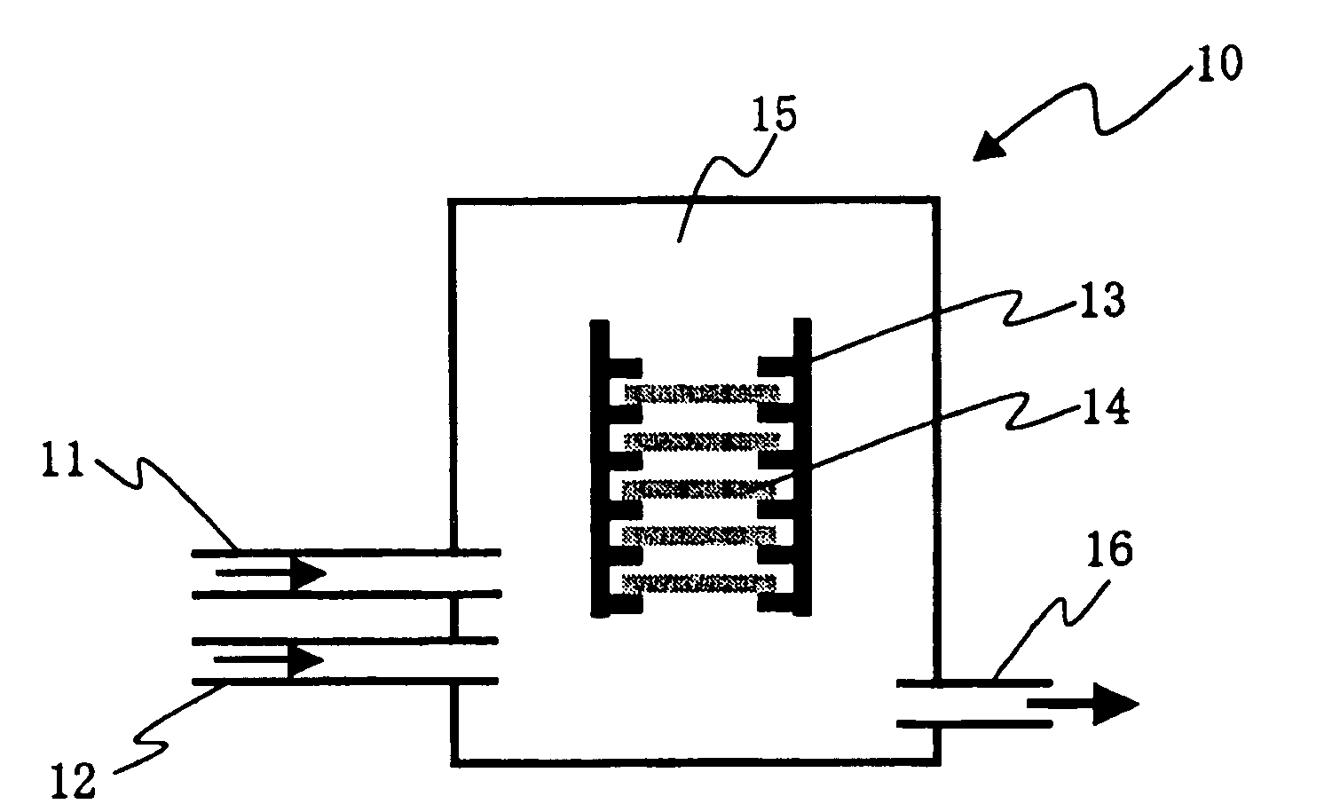
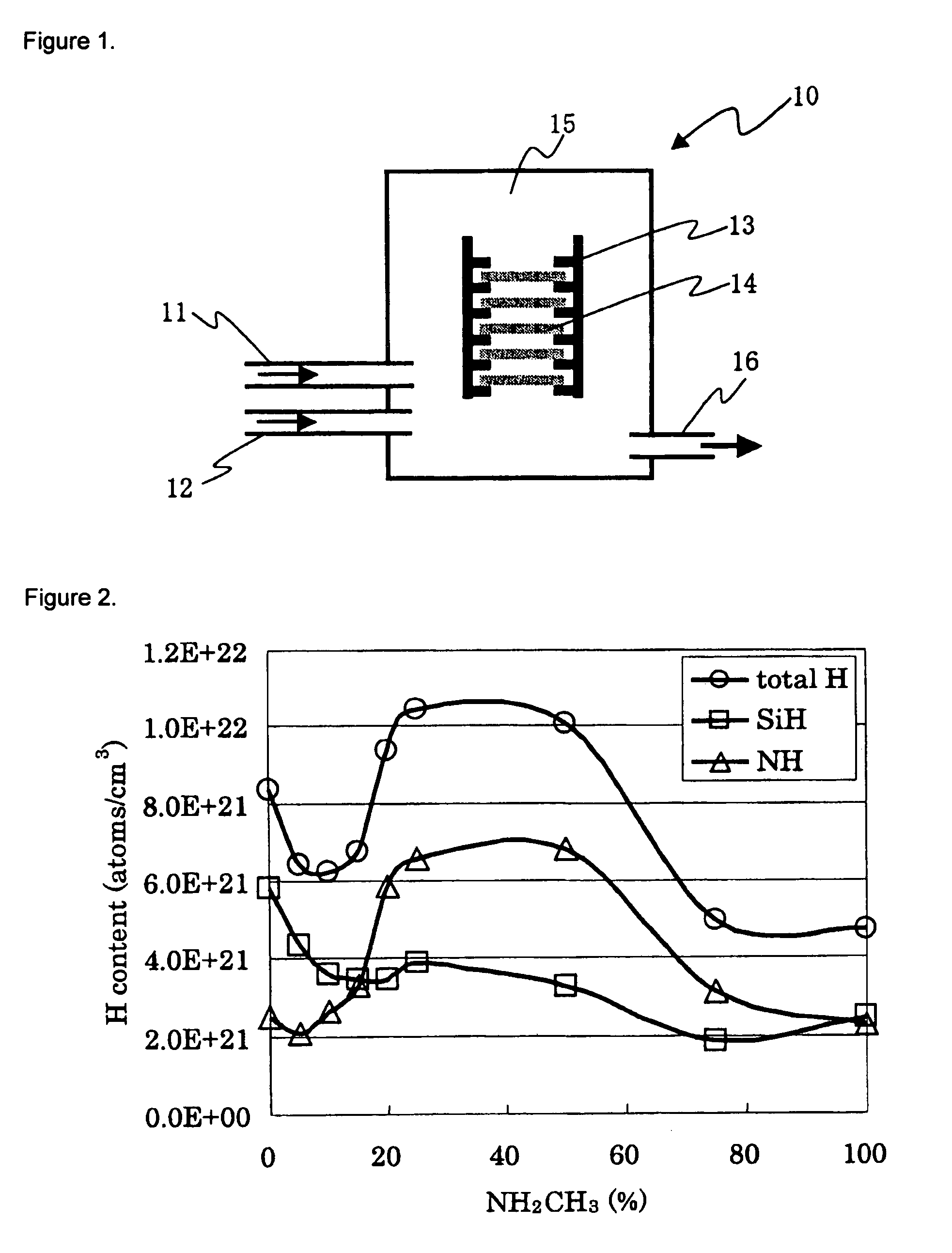
[0038]FIG. 1 illustrates an LPCVD tool for executing the method according to the present invention for forming silicon nitride films. Silicon source (SiH2Cl2, SiCl4, Si2Cl6, etc.) gas is fed into this LPCVD tool 10 from the injector 11; a mixed gas of monomethylamine (CH3NH2) and ammonia (NH3) as nitrogen source is fed from the injector 12; and a silicon nitride film is formed on the silicon wafer 14 that is mounted in the boat 13 in the reaction compartment 15. Reference symbol 16 refers to an exhaust port.

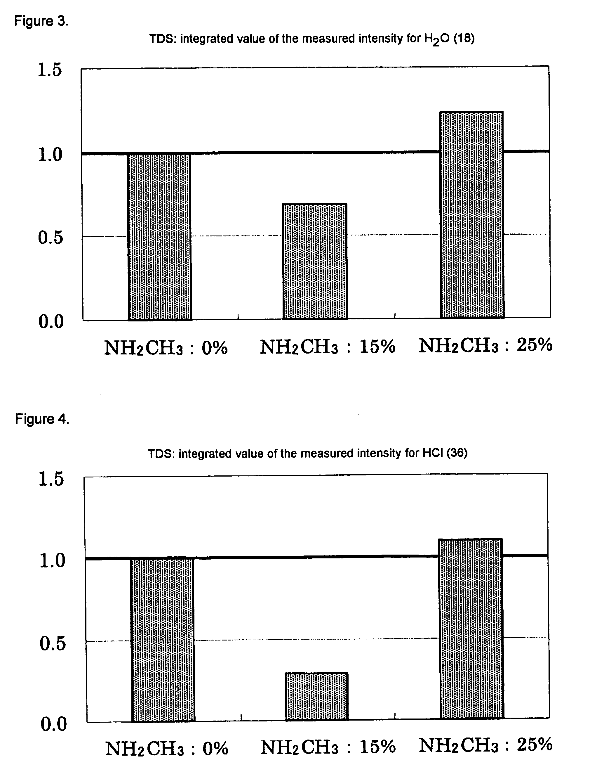
[0039] The addition of the monomethylamine makes it possible to terminate the silicon dangling bonds with the methyl group and thereby enables an improvement in the film quality and leakage characteristics, etc., even at low temperatures (450-600° C.). While low temperatures (450-600° C.) are identified for the film-formation temperature, the film-formation temperature is not limited to these temperatures. That is silicon nitride film with good film properties and good leakage c...

example 2

[0056] FIGS. 8(a) through (d) contain process cross sections that illustrate an example of the application of the inventive silicon nitride film to a MOSFET (dielectric gate transistor).

[0057] As shown in FIG. 8(a), an element isolation region 72 comprising a dielectric (e.g., SiO2) is formed on a silicon substrate 71 and a MOSFET 70 is formed in the region defined by the element-forming regions. This MOSFET 70 is constituted of source and drain extension regions 73a, 73b (denoted below as SD extensions) that have been ion-implanted with boron (B), a source region 74a and drain region 74b corresponding to these SD extensions, and a gate electrode 77 separated by an intervening gate dielectric film 76.

[0058] A channel region 75 is formed between the SD extensions in this MOSFET 70, while a sidewall film 78 is formed on the sidewall surfaces of the gate dielectric film 76 and gate electrode 77. This sidewall film 78 comprises Si3N4 film and is formed using the LPCVD tool shown in FI...


PUM

PropertyMeasurementUnit
Temperatureaaaaaaaaaa

Abstract

Silicon nitride film is formed on a silicon wafer mounted in a boat in an LPCVD tool by feeding a silicon source (SiH2Cl2, SiCl4, Si2Cl6, etc.) from an injector and feeding a mixed gas of monomethylamine (CH3NH2) and ammonia (NH3) as the nitrogen source from an injector. This addition of monomethylamine to the source substances for film production makes it possible to provide an improved film quality and improved leakage characteristics even at low temperatures (450-600° C.).

Description

TECHNICAL FIELD [0001] This invention relates to a method for producing silicon nitride films and to a process for fabricating semiconductor devices using said method. BACKGROUND ART [0002] When the fabrication of silicon nitride film is carried out by the generally known low-pressure chemical vapor deposition (LPCVD) procedure using ammonia (NH3) and a silicon source such as dichlorosilane (SiH2Cl2), tetrachlorosilane (SiCl4), or hexachlorodisilane (Si2Cl6), a substantial deterioration in leakage characteristics and wet etching resistance is noted when the film production temperature declines below, for example, 600° C. It is thought that the generation of silicon-nitrogen bonds by reaction between the silicon source and nitrogen source is not promoted in such a low-temperature film-formation process and that the resulting occurrence of a large number of silicon dangling bonds in the silicon nitride film causes the deterioration in film quality. [0003] The use of monomethylamine (C...

Claims


Application Information

Patent Timeline
IPC IPC(8): C23C16/34H01L21/318
CPCH01L21/3185C23C16/345H01L21/02271H01L21/02211H01L21/0217
Inventor HOSHI, TAKESHISAITO, TSUYOSHIKIMURA, TAKAKODUSSARRAT, CHRISTIANYANAGITA, KAZUTAKA
Owner LAIR LIQUIDE SA POUR LETUDE & LEXPLOITATION DES PROCEDES GEORGES CLAUDE
Why Eureka
Try Eureka