Piezoelectic element and method for manufacturing the same, and ink jet head and ink jet recording apparatus using the piezoelectric element

a piezoelectric element and piezoelectric technology, applied in the field of piezoelectric element and method for manufacturing the same, and ink jet head and ink jet recording apparatus using piezoelectric element, can solve the problems of dielectric breakdown, reduced insulation resistance, and decreased piezoelectric insulation of piezoelectric material

Active Publication Date: 2005-07-28
PANASONIC CORP
View PDF2 Cites 32 Cited by
  • Summary
  • Abstract
  • Description
  • Claims
  • Application Information

AI Technical Summary

Benefits of technology

[0045] Then, an ink jet recording apparatus of line head type is obtained easily.

Problems solved by technology

However, if a high voltage is applied to the piezoelectric element that has been subjected to a high humidity atmosphere for a long time, the electrical insulation of the piezoelectric material is decreased, resulting in a dielectric breakdown.
This phenomenon has been one of the major problems in achieving the reliability of the piezoelectric element.
In other words, this insulation resistance decrease results from the fact that water directly attacks the piezoelectric material.
However, in the above method, since zirconia processing or the like has to be performed after the formation of the layered structure, the fabrication process becomes complicated.

Method used


Image

  • Piezoelectic element and method for manufacturing the same, and ink jet head and ink jet recording apparatus using the piezoelectric element
  • Piezoelectic element and method for manufacturing the same, and ink jet head and ink jet recording apparatus using the piezoelectric element
  • Piezoelectic element and method for manufacturing the same, and ink jet head and ink jet recording apparatus using the piezoelectric element

Examples


first embodiment

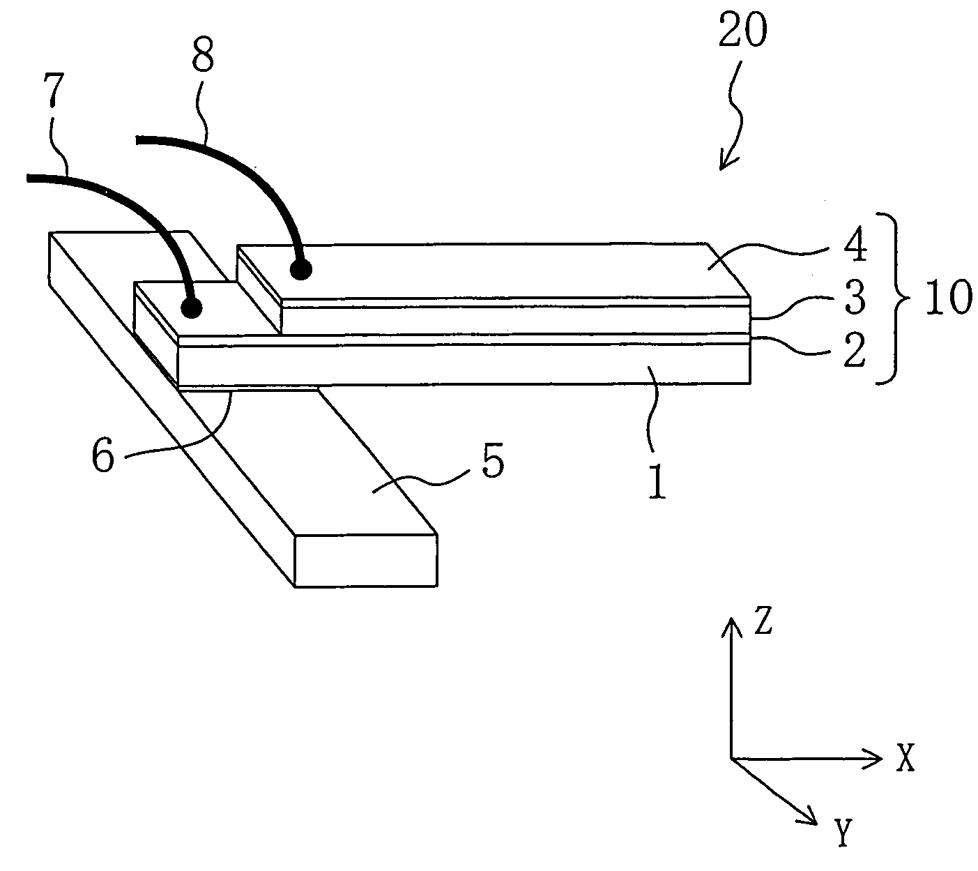
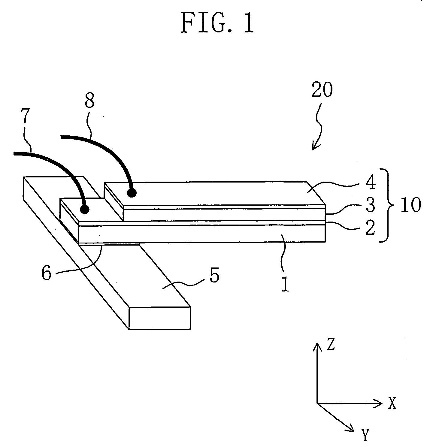
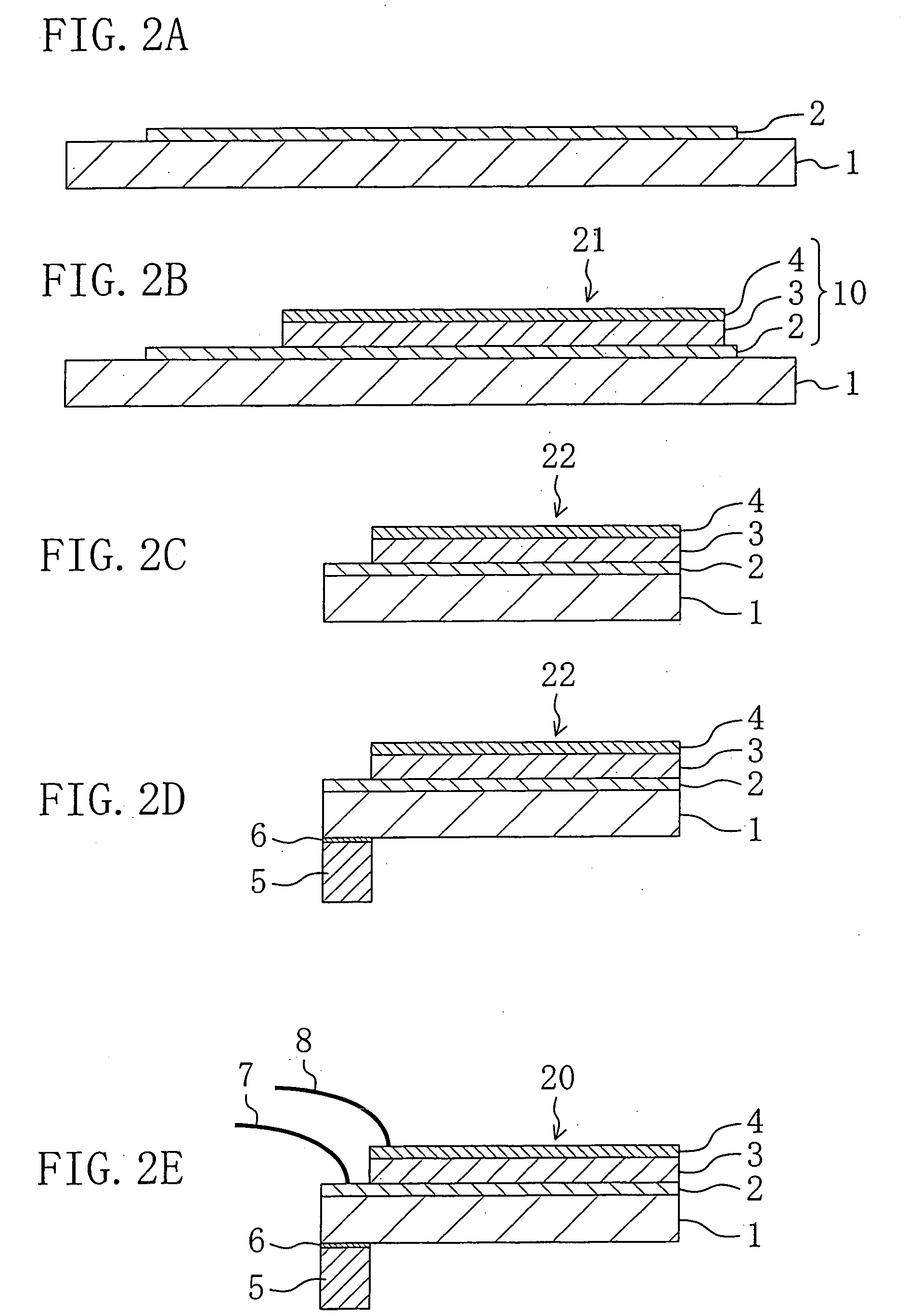
[0056]FIG. 1 is a perspective view illustrating a piezoelectric element according to an embodiment of the present invention. As illustrated in FIG. 1, the piezoelectric element 20 of this embodiment includes a substrate 1 made of flat strip shaped silicon (Si) having a length of 11.0 mm, a width of 3.0 mm, and a thickness of 0.30 mm, and a layered structure 10 provided on the substrate 1. A 3.0-mm end portion of the piezoelectric element 20 is fixed, via an epoxy adhesive 6, to a stainless steel support substrate 5 having a length of 10.0 mm, a width of 3.0 mm, and a thickness of 1.0 mm and extending in the direction perpendicular to the piezoelectric element 20 (i.e., the Y axis direction in the coordinate system of FIG. 1). The piezoelectric element 20 is supported by the stainless steel support substrate 5 to form a cantilever.

[0057] The layered structure 10 includes a first electrode film 2, a piezoelectric thin film 3, and a second electrode film 4 layered in this order, and i...

example 1

[0077] A substrate 1 was a silicon substrate having the same shape as that employed in the above-described embodiment. As in the above embodiment, a first electrode film 2 was an iridium alloy thin film having a thickness of 0.10 μm and containing 6 mol % of cobalt. Using an RF magnetron sputtering apparatus, the iridium alloy thin film was deposited through a sputtering process by applying a high-frequency power of 200 W to a 6 mol %-cobalt-containing iridium plate serving as the target of the sputtering apparatus for 16 minutes, while keeping the temperature of the silicon substrate at 400° C. in a mixed gas of argon and oxygen (gas volume ratio: Ar:O2=15:1) serving as the sputtering gas at a total gas pressure of 0.25 Pa. In this film deposition process, in the sputtering apparatus, the potential of the silicon substrate was kept electrically floating so as not to be fixed at the ground potential.

[0078] A piezoelectric thin film 3 was a PZT thin film preferentially oriented alon...

example 2

[0090] In this example, the sputtering gas pressure, a sputtering deposition condition employed in formation of a piezoelectric thin film 3 (PZT thin film), was changed to 0.12 Pa, and in the other respects, a piezoelectric element 20 was prepared in the same manner as in Example 1.

[0091] As a result of an analysis by an X-ray diffraction method, it was found that the PZT thin film of the piezoelectric element 20 obtained in this manner was a film having a perovskite crystalline structure and preferentially oriented along the (001) plane (the (001) crystalline orientation degree was 96%). Moreover, results of a composition analysis with an X-ray microanalyzer showed that the composition of the PZT thin film was expressed by Pb(1−x)(Zr(1−s)Tis)O3 where x=0.03 (i.e., Pb0.97(Zr0.53Ti0.47)O3). Furthermore, as a result of observation by a scanning electron microscope, it was found that the thickness of the PZT thin film was 3.5 μm.

[0092] Then, a triangular voltage with a maximum voltag...


PUM

PropertyMeasurementUnit
thicknessaaaaaaaaaa
thicknessaaaaaaaaaa
pressureaaaaaaaaaa

Abstract

A lead content in a piezoelectric thin film (3) of a piezoelectric element (20) is made smaller as compared to stoichiometric composition. More specifically, the piezoelectric thin film (3) is made of lead zirconate titanate expressed as Pb(1−x)(Zr(1−s)Tis)O3(0<s<1) or lead-zirconate-titanate-based oxide expressed as (Pb(1−x−y)Ay)(Zr(1−t)TisBt)O3(0<s<1, 0<t<1−s) where A is a substitutive metal ion in an A-site in the perovskite crystalline structure and B is a substitutive metal ion in a B-site in the perovskite crystalline structure. The value of x, which indicates a deficiency in Pb content in each composition, is more than 0 but not more than 0.15.

Description

CROSS-REFERENCE TO RELATED APPLICATION [0001] The disclosure of Japanese Patent Application No. 2004-018017 filed on Jan. 27, 2004 including specification, drawings and claims is incorporated herein by reference in its entirety. BACKGROUND OF THE INVENTION [0002] 1. Field of the Invention [0003] The present invention relates to a piezoelectric element having an electro-mechanical conversion function and a method for manufacturing the same, and an ink jet head and an ink jet recording apparatus using the piezoelectric element. [0004] 2. Description of the Prior Art [0005] Generally, a piezoelectric element has a layered structure in which a piezoelectric material is interposed between two electrodes in the thickness direction. A piezoelectric material is made of a material capable of converting a mechanical energy to an electrical energy and vice versa. Typical examples of a piezoelectric material include lead zirconate titanate (Pb(Zr,Ti)O3) (hereinafter referred to as “PZT”), which...

Claims


Application Information

Patent Timeline
Patent Type & Authority Applications(United States)
IPC IPC(8): B41J2/14B41J2/16H01L41/09H01L41/18H01L41/316
CPCB41J2/161B41J2/1623B41J2/1628B41J2/1631B41J2/1632H01L41/316B41J2/1646B41J2002/1425H01L41/0805H01L41/094H01L41/1876B41J2/1642H10N30/1051H10N30/2042H10N30/8554H10N30/076
Inventor TORII, HIDEOFUJII, EIJIKAMADA, TAKESHI
Owner PANASONIC CORP
Why Eureka
Try Eureka