

Method for manufacturing a semiconductor device
a manufacturing method and semiconductor technology, applied in the direction of semiconductor devices, electrical devices, transistors, etc., can solve the problems of reducing the data retention characteristic of memory cells, increasing junction leakage current, and reducing the electric field strength, so as to reduce the number of crystal defects remaining after heat treatment, reduce the acceleration energy for implantation, and reduce the damage in the crystal structure of the substrate
- Summary
- Abstract
- Description
- Claims
- Application Information
AI Technical Summary
Benefits of technology
Problems solved by technology
Method used
Image

Examples
first embodiment
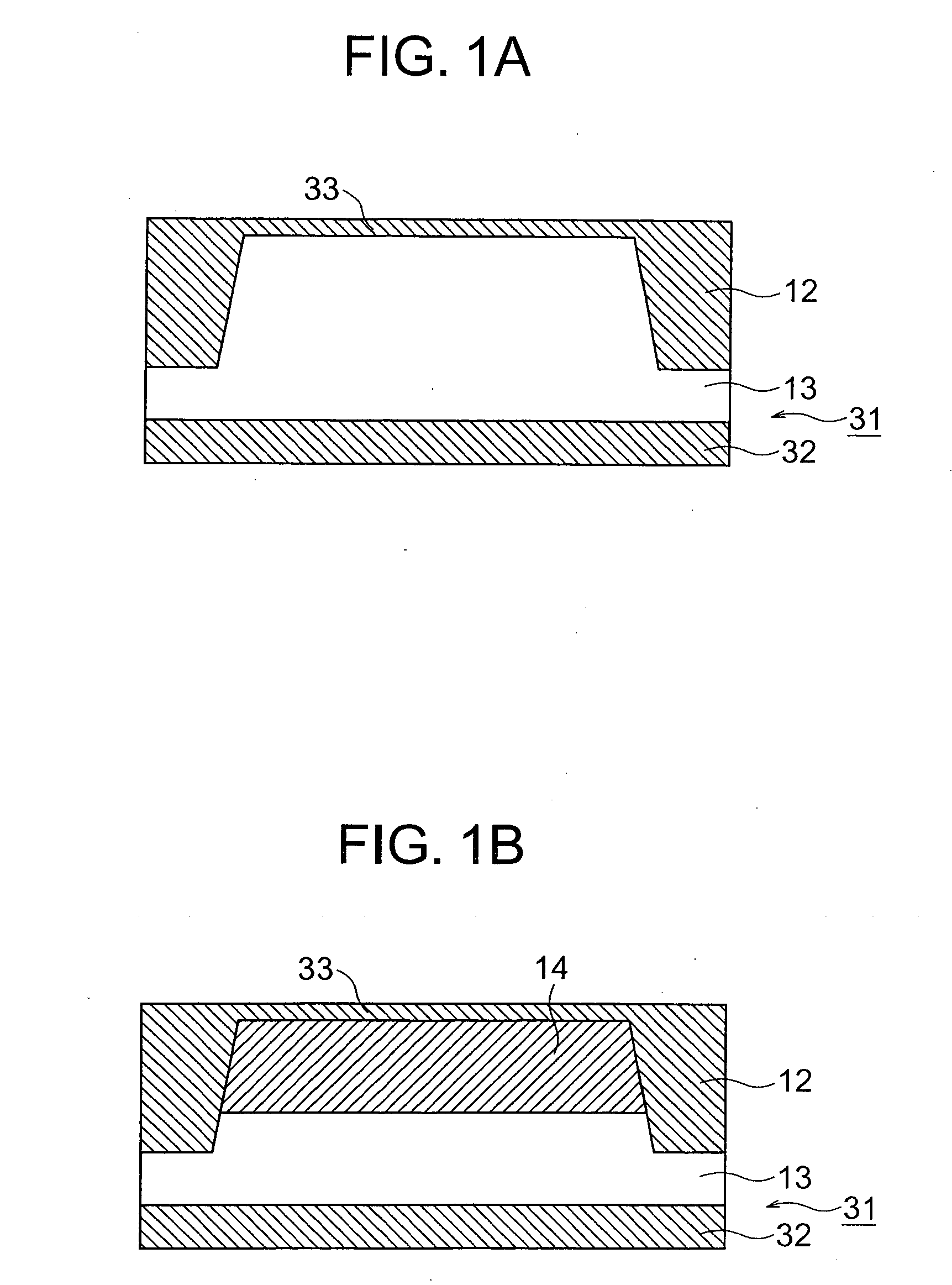
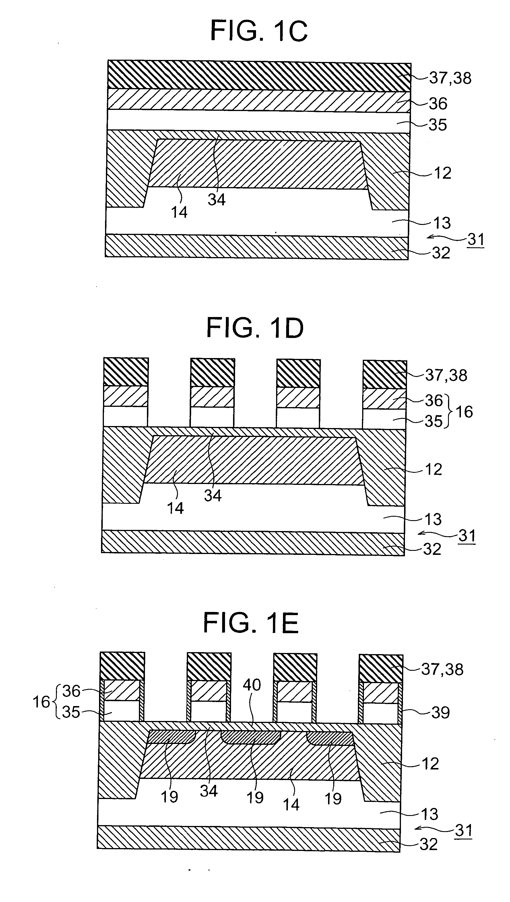
[0040] Hereinafter, the present invention will be described in more detail based on preferred embodiments according to the present invention. FIGS. 1A to 1G and FIG. 2 are sectional views respectively showing the steps of manufacturing a semiconductor device according to the present invention, wherein the present invention is applied to manufacture of cell transistors in a DRAM.
[0041] As shown in FIG. 1A, shallow trenches are first formed in the main surface of a silicon substrate 31. Thereafter, an insulating film 12 is filled in the shallow trenches to form shallow-trench isolation regions. Subsequently, a silicon oxide film 33 having a thickness of 10 nm is formed on the substrate surface. Through the silicon oxide film 33, phosphorus implantation is carried out at an acceleration energy of 1000 keV and a dosage of 1×10¹³ / cm2. Subsequently, a heat treatment is carried out at a substrate temperature of 1000° C. for 10 minutes in a nitrogen ambient, to form an n-type buried well la...
second embodiment
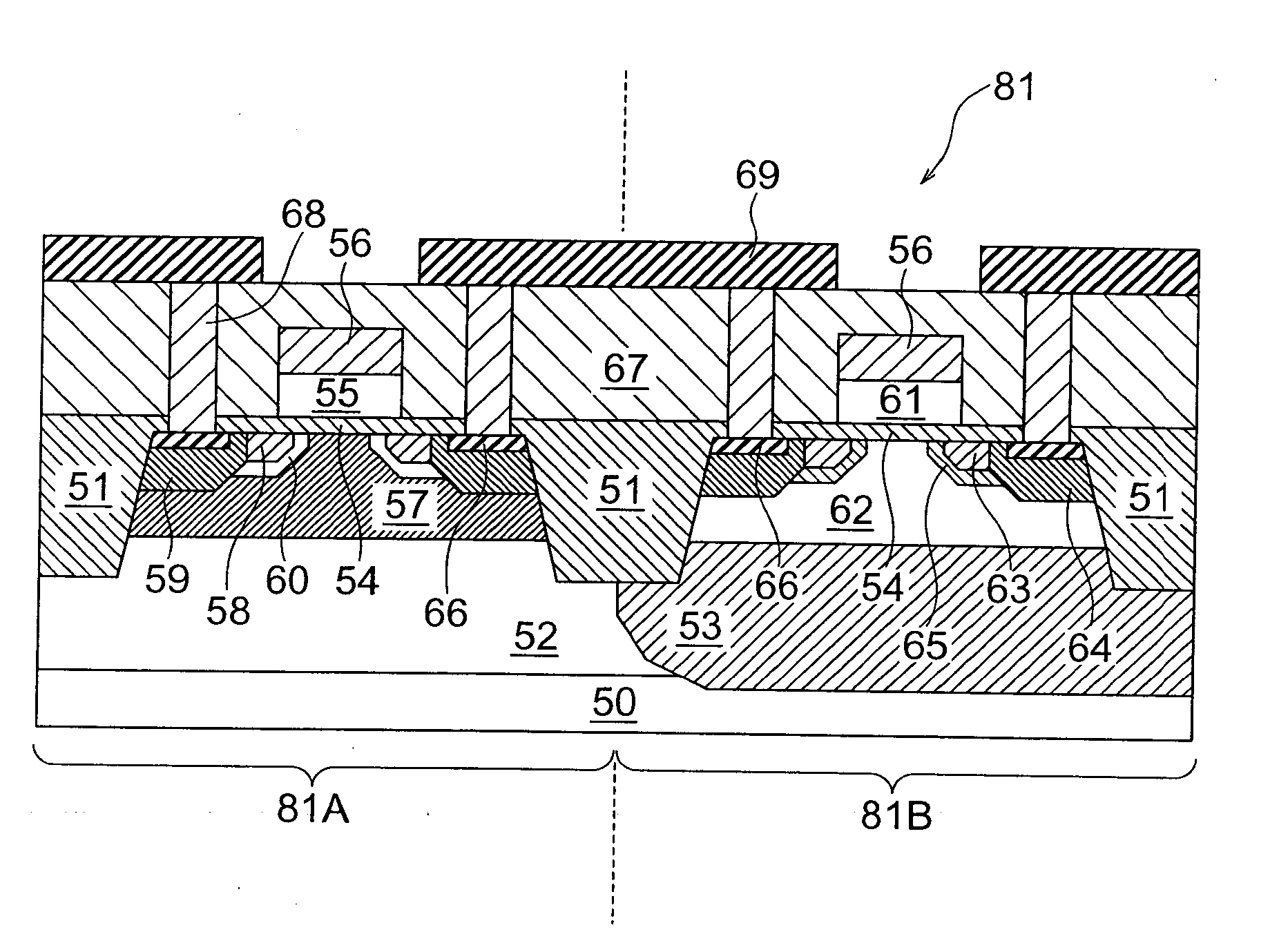
[0060]FIGS. 5A to 5K are sectional views respectively showing manufacturing steps in a method for manufacturing a semiconductor device, according to the present invention. As shown in FIG. 5A, the element isolation regions 51 are first formed by use of a well-known method. Thereafter, a silicon oxide film 71 having a thickness of 10 nm is formed on the surface of the substrate 50.
[0061] Next, boron is implanted in three steps through the silicon oxide film 71, to form a p-type well layer 52. More specifically, the p-type well layer 52 is formed by implanting boron in a first-step implantation at an acceleration energy of 300 KeV and a dosage of 1×10¹³ / cm2 and then carrying out a heat treatment at a substrate temperature of 1000° C. for 10 minutes in a nitrogen ambient. Subsequently, a second-step boron implantation is performed two times, at an acceleration energy of 150 KeV and a dosage of 5×10¹² / cm2 and then at an acceleration energy of 50 KeV and a dosage of 1×10¹³ / cm2. Thereafte...
PUM
 Abstract
Description
Claims
Application Information