Thermal interface material and method for manufacturing same

a technology of thermal interface materials and manufacturing methods, which is applied in the direction of solid-state devices, basic electric elements, chemistry apparatuses and processes, etc., can solve the problems of inadequate heat dissipation requirements of modem electronic components, the heat conduction coefficient is now considered too low for many contemporary applications, and the value of the heat conduction coefficient cannot be increased, so as to reduce the thickness, small thermal interface resistance, and good flexibility

Active Publication Date: 2005-08-04
TSINGHUA UNIV +1
View PDF5 Cites 135 Cited by
  • Summary
  • Abstract
  • Description
  • Claims
  • Application Information

AI Technical Summary

Benefits of technology

[0011] Accordingly, an object of the present invention is to provide a thermal interface material having a reduced thickness, small thermal interface resistance, good flexibility and excellent heat conduction.
[0019] Unlike in a conventional thermal interface material, the carbon nanotubes of the thermal interface material of the present invention are disposed in the macromolecular material uniformly and directionally. Thus, each carbon nanotube of the thermal interface material can provide a heat conduction path in a direction perpendicular to a main heat absorbing surface of the thermal interface material. This ensures that the thermal interface material has a high heat conduction coefficient. Furthermore, the thickness of the thermal interface material of the present invention can be controlled by cutting the macromolecular material. This further enhances the heat conducting efficiency of the thermal interface material and reduces the volume and weight of the thermal interface material. Moreover, each carbon nanotube is open at two ends thereof, and extends from the first surface to the second surface of the thermal interface material. This ensures the carbon nanotubes can contact an electronic device and a heat sink directly. Thus, the thermal interface resistance between the carbon nanotubes and the electronic device is reduced, and the thermal interface resistance between the carbon nanotubes and the heat sink is reduced. Therefore, the heat conducting efficiency of the thermal interface material is further enhanced.

Problems solved by technology

However, a heat conduction coefficient of the thermal interface material is now considered to be too low for many contemporary applications, because it cannot adequately meet the heat dissipation requirements of modem electronic components.
The value of the heat conduction coefficient cannot be increased, because the thickness cannot be reduced.
However, the thermal interface material formed by injection molding is relatively thick.
This increases a bulk of the thermal interface material and reduces its flexibility.
This means that heat does not necessarily spread uniformly through the thermal interface material.

Method used


Image

  • Thermal interface material and method for manufacturing same
  • Thermal interface material and method for manufacturing same

Examples


Embodiment Construction

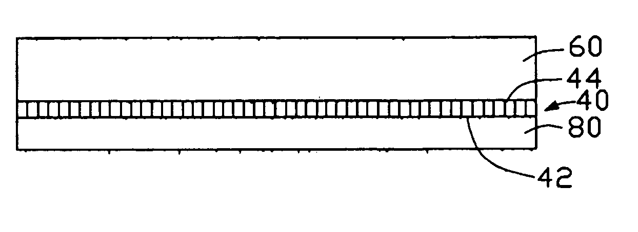
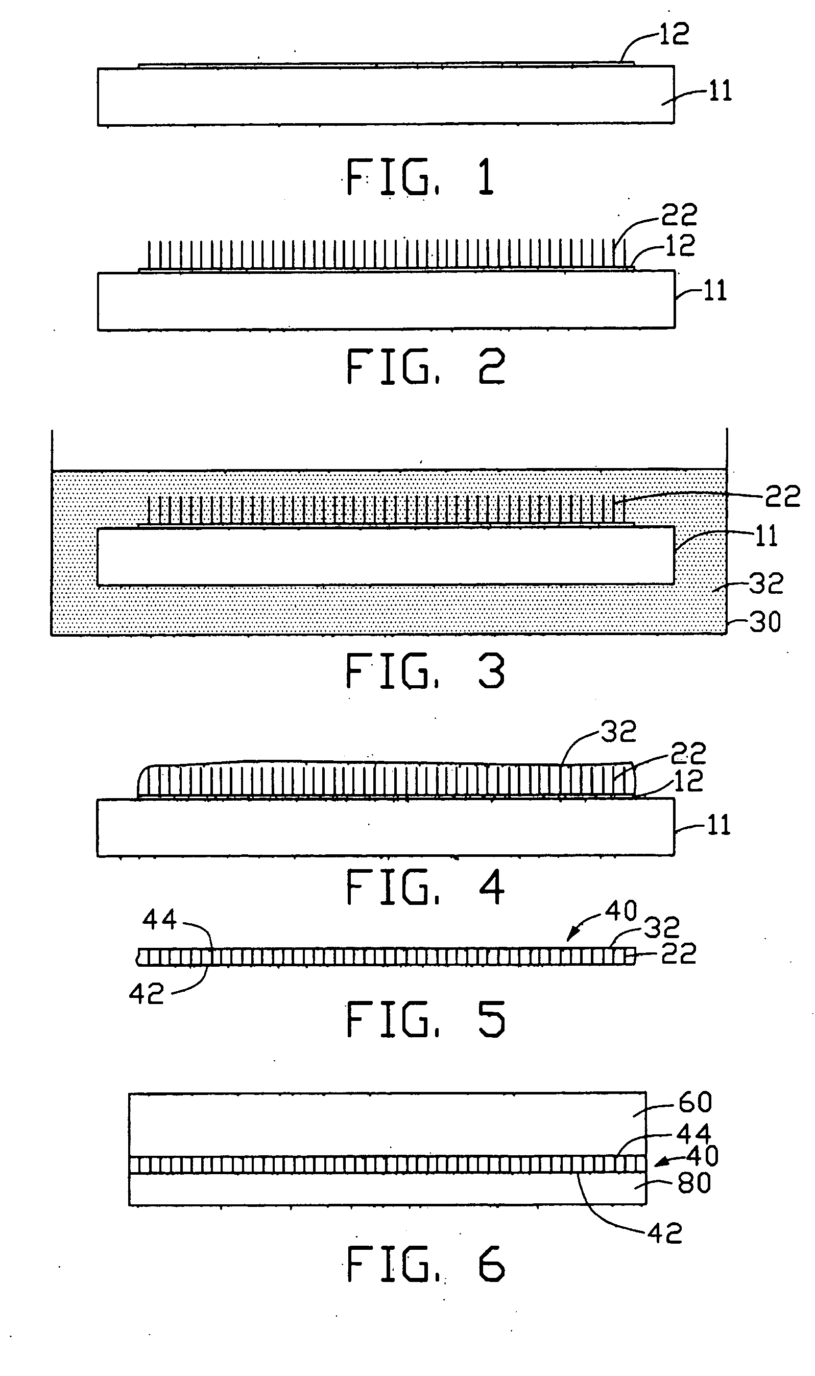
[0027] Referring to FIG. 1, a substrate 11 having a catalyst film 12 attached thereon is shown. In FIG. 2, an array of carbon nanotubes 22 directionally formed on the substrate 11 is shown. The carbon nanotubes 22 are manufactured by way of thermal chemical vapor deposition or plasma enhanced chemical vapor deposition. In a preferred method of the present invention, the carbon nanotubes 22 are manufactured as follows. Firstly, the substrate 11 is provided. The substrate 11 can be made of glass, quartz, silicon, or alumina. In the preferred embodiment, the substrate 11 is made of porous silicon. A surface of the porous silicon is a porous layer. Diameters of apertures in the porous layer are extremely small, generally about 3 nanometers. Then the catalyst film 12 is uniformly disposed on the substrate 11 by chemical vapor deposition, thermal disposition, electron-beam disposition, or sputtering. The catalyst film 12 can be made of iron (Fe), cobalt (Co), nickel (Ni), or an alloy ther...


PUM

PropertyMeasurementUnit
thicknessaaaaaaaaaa
thicknessaaaaaaaaaa
temperatureaaaaaaaaaa

Abstract

A thermal interface material (40) includes a macromolecular material (32), and a plurality of carbon nanotubes (22) embedded in the macromolecular material uniformly. The thermal interface material includes a first surface (42) and an opposite second surface (44). Each carbon nanotube is open at both ends thereof, and extends from the first surface to the second surface of the thermal interface material. A method for manufacturing the thermal interface material includes the steps of: (a) forming an array of carbon nanotubes on a substrate; (b) submerging the carbon nanotubes in a liquid macromolecular material; (c) solidifying the liquid macromolecular material; and (d) cutting the solidified liquid macromolecular material to obtain the thermal interface material with the carbon nanotubes secured therein.

Description

BACKGROUND OF THE INVENTION [0001] 1. Field of the Invention [0002] The invention relates generally to thermal interface materials and manufacturing methods thereof; and more particularly to a thermal interface material which conducts heat by using carbon nanotubes, and a manufacturing method thereof. [0003] 2. Description of Related Art [0004] Electronic components such as semiconductor chips are becoming progressively smaller, while at the same time heat dissipation requirements thereof are increasing. Commonly, a thermal interface material is utilized between the electronic component and a heat sink in order to efficiently dissipate heat generated by the electronic component. [0005] A conventional thermal interface material is made by diffusing particles with a high heat conduction coefficient in a base material. The particles can be made of graphite, boron nitride, silicon oxide, alumina, silver, or other metals. However, a heat conduction coefficient of the thermal interface ma...

Claims


Application Information

Patent Timeline
Patent Type & Authority Applications(United States)
IPC IPC(8): B29C70/10C08K3/04C08K7/08C08L83/00C09K5/14H01L21/76H01L23/373H01L31/0328
CPCB82Y30/00H01L23/373Y10S977/742Y10S977/842Y10S977/712Y10S977/856Y10S977/855H01L2924/0002Y10S977/735Y10S977/848Y10S977/743H01L2924/00
Inventor HUANG, HUALIU, CHANG-HONGFAN, SHOU-SHAN
Owner TSINGHUA UNIV
Why Eureka
Try Eureka