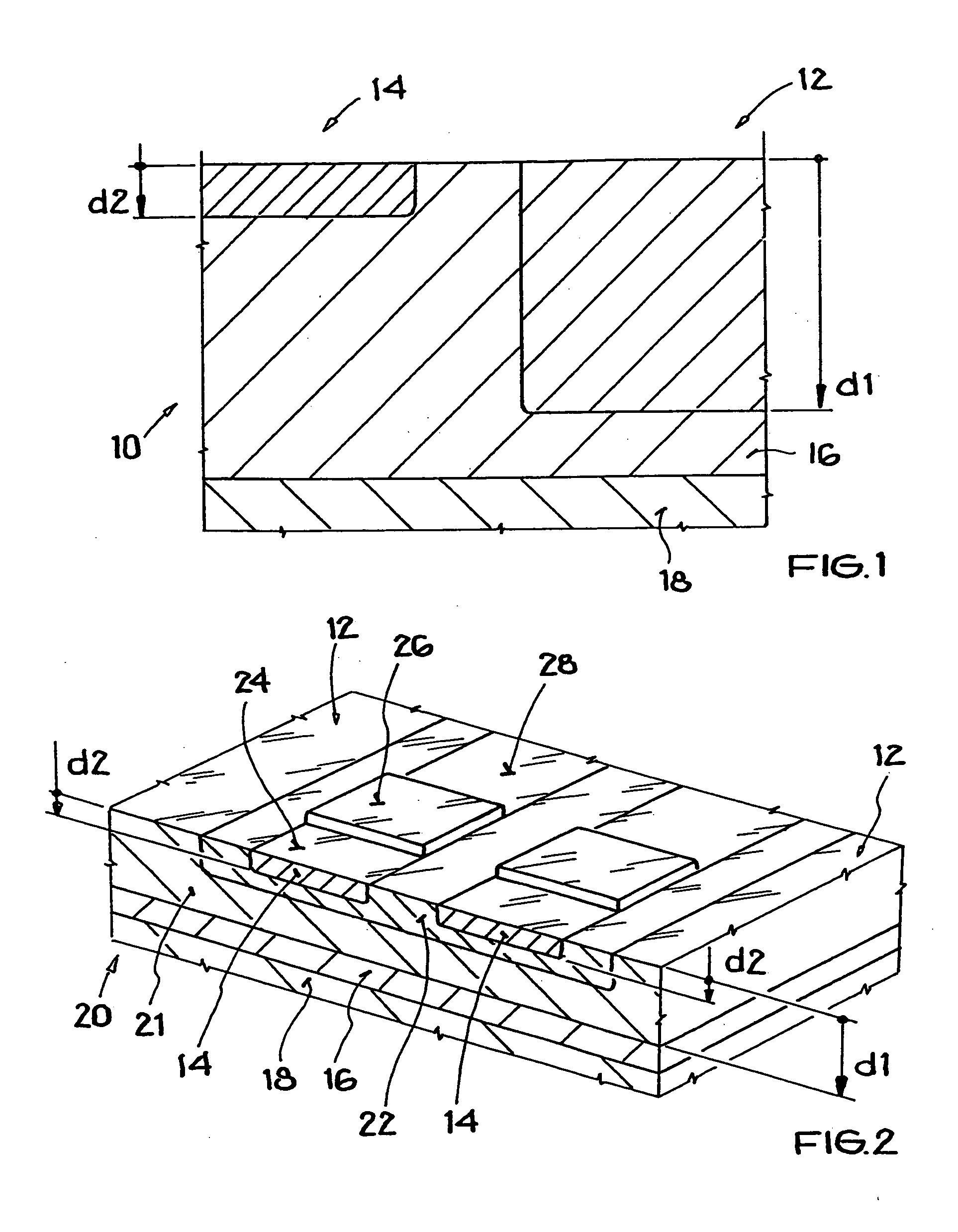
[0022] The inventive method enables a simultaneous integration of low power
CMOS and high power DMOS (so-called “ultra
smart power”) on regions or portions of active semiconductor material respectively having different thicknesses. Through the use of an SOI wafer, it is possible to integrate DMOS elements on a thick
SOI substrate and
CMOS elements on a thin
SOI substrate using a common SOI technology on a single common wafer with maximum packing density. The active semiconductor material that is overgrown in the context of the inventive method has no connection to the substrate, so that a complete electrical decoupling or
dielectric isolation of the thin active semiconductor
layers from the substrate can be achieved. Another
advantage of the invention is that the seed openings for the selective
epitaxy are formed independent of lithographic processes, whereby space is saved and a higher integration density is achieved. Overall, the inventive method reduces an increase of leakage currents that are expected in connection with a scaled reduction of the structural width.
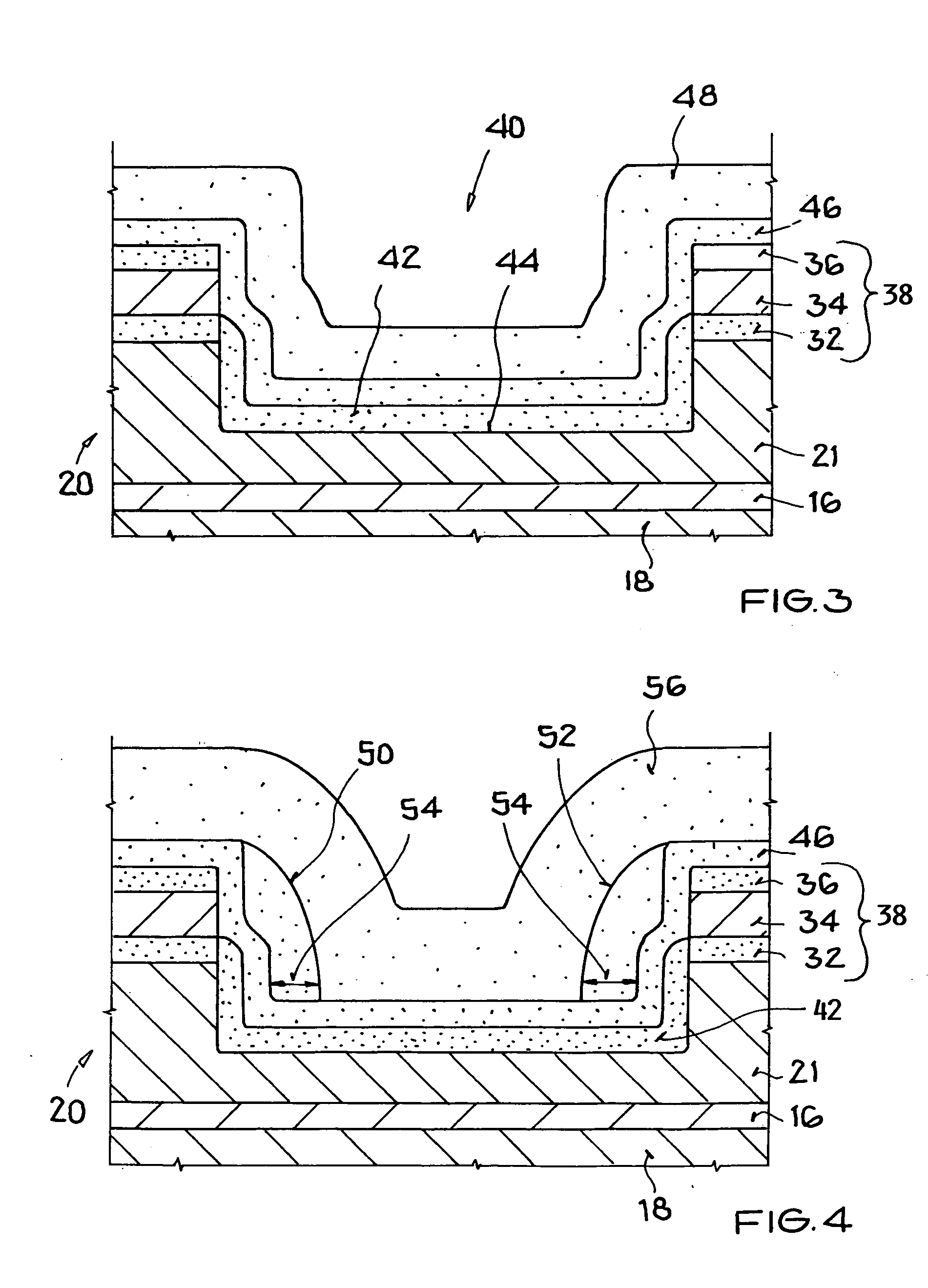
[0023] It is preferred according to the invention that the trench is produced by means of a
shallow trench isolation (STI)
etching technology, which involves an
anisotropic etching process to form an etched trench between active regions that have been covered with a
nitride protective layer, and then the trench is filled with an insulating material such as
silicon dioxide or polysilicon. Thereby, the STI technology is able to achieve high packing densities.
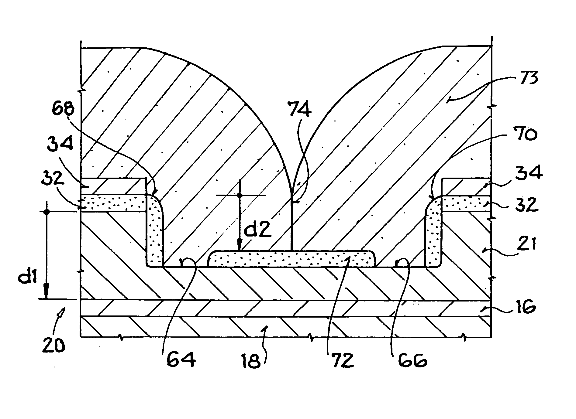
[0024] It is further preferred that the step or process of producing spacers at the sides within the trench structure on the first
oxide layer involves the following sub-steps: covering the trench including the inner wall areas of the trench with a
polycrystalline semiconductor material, and then anisotropically
etching away the
polycrystalline semiconductor material from the central floor area of the trench, so that only spacers of the
polycrystalline semiconductor material remain along the inner wall regions of the trench.
[0025] In view of the above, it is apparent that the material for the spacers is provided by the covering of the trench structure. Further in this regard, an
etching process is regarded as anisotropic when the etching front progresses in a certain
spatial direction more quickly than in other spatial directions. As a result of a more-rapid etching process in the vertical direction, thereby
polycrystalline material will preferentially remain in place along the wall areas of the trench throughout and after the vertical
anisotropic etching progresses vertically toward the trench floor. Thus, the remaining
polycrystalline material along the trench sidewalls forms the desired poly-spacers. The width of the thusly produced poly-spacers will define the width of the seed openings to be formed in the trench for the following selective
epitaxy. In this manner, it is possible to produce seed openings with nearly any desired arbitrarily small dimensions, for example also for technologies with a limited structural resolution. In this context, the term “seed” refers to the exposed
surface structure of a monocrystal on which atoms will be deposited and begin to grow in the ELO process, such that the
crystal material epitaxially grown in the ELO process will take on or mimic the
crystal orientation of the
seed crystal, i.e. the exposed surface of the underlying monocrystal.
[0026] According to a further preferred feature, the step of filling the trench with a second
oxide layer between the spacers involves depositing a tetraethylorthosilicate (TEOS) oxide. In this regard,
silicon dioxide is produced through the
decomposition of the TEOS compound at moderate temperatures (e.g. up to about 700° C.). This process is also referred to as TEOS
pyrolysis, and results in high-value, high-quality oxide films, which are characterized, for example, by a high breakdown or breakthrough
field strength and a conforming edge covering ability.
[0027] It is also preferred that the step of covering the SOI wafer with a protective layer especially includes the following sub-steps: covering the SOI wafer with a first oxide partial layer; covering the first oxide partial layer with a
nitride layer; and covering the
nitride layer with a second oxide partial layer. This layering process sequence produces a so-called oxide-nitride-oxide (ONO) layer, which is used as a
hard mask in the etching process for forming the trench. In comparison to a “soft”
lacquer or
resist mask, the use of such a
hard mask achieves improved accuracy with which the angles and the shape of the sidewalls of the trench are produced. Moreover, during the later covering of the trench with an oxide layer, the nitride layer of the ONO multilayer prevents an undesired oxidation of areas of the surface of the layer of active semiconductor material
lying outside of the trench.

