Heterojunction structure of nitride semiconductor and nano-device or an array thereof comprising same

a technology of nitride semiconductor and nano-device, which is applied in the direction of semiconductor devices, electrical devices, nanotechnology, etc., can solve the problems of high manufacturing cost and relatively low luminescence efficiency, and achieve low cost, high light-emission properties, and facilitate electron tunneling

Inactive Publication Date: 2005-08-18
POSTECH ACAD IND FOUND
View PDF4 Cites 79 Cited by
  • Summary
  • Abstract
  • Description
  • Claims
  • Application Information

AI Technical Summary

Benefits of technology

[0004] Accordingly, it is an object of the present invention to provide a novel nitride-based structure which can be formed on a substrate other than sapphire and

Problems solved by technology

Such light emitting devices, however, comprise a gallium nitride in the form of a thin film deposited on a sa

Method used


Image

  • Heterojunction structure of nitride semiconductor and nano-device or an array thereof comprising same
  • Heterojunction structure of nitride semiconductor and nano-device or an array thereof comprising same
  • Heterojunction structure of nitride semiconductor and nano-device or an array thereof comprising same

Examples


example 1

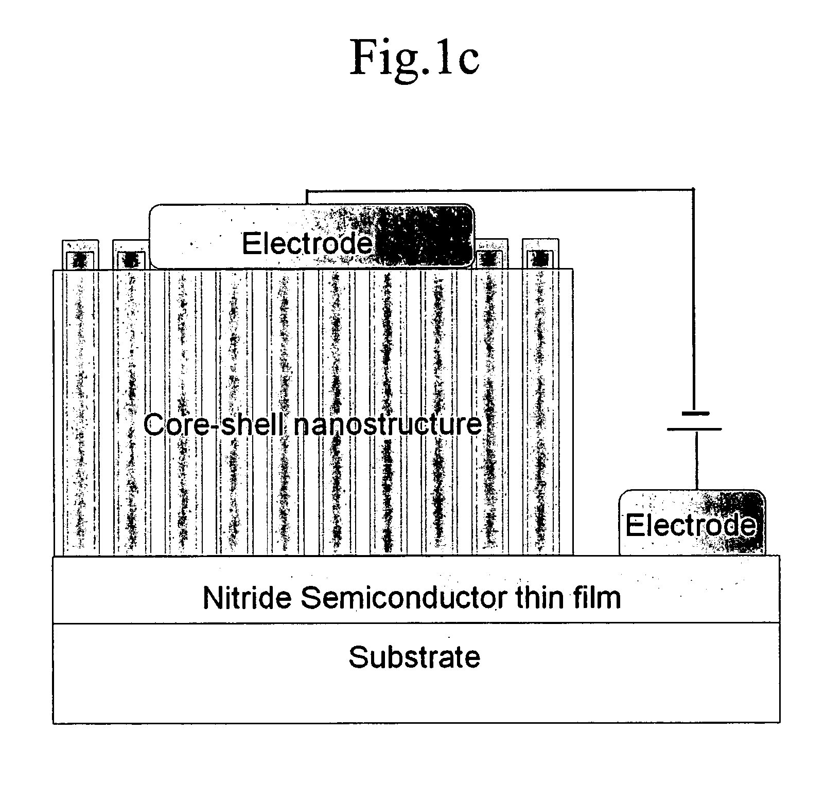
The Growth of Core-shell Nanostructures on a Nitride Semiconductor Thin Film

[0027] An Mg-doped GaN thin film was deposited on an Al2O3 substrate using a conventional MOCVD technique and annealed, to obtain a p-type GaN thin film having a thickness of 2 μm. The metal organic precursors used were trimethylgallium (TMGa) and bis(cyclopentadienyl) magnesium ((C5H5)2Mg); and the nitrogen precursor, NH3.

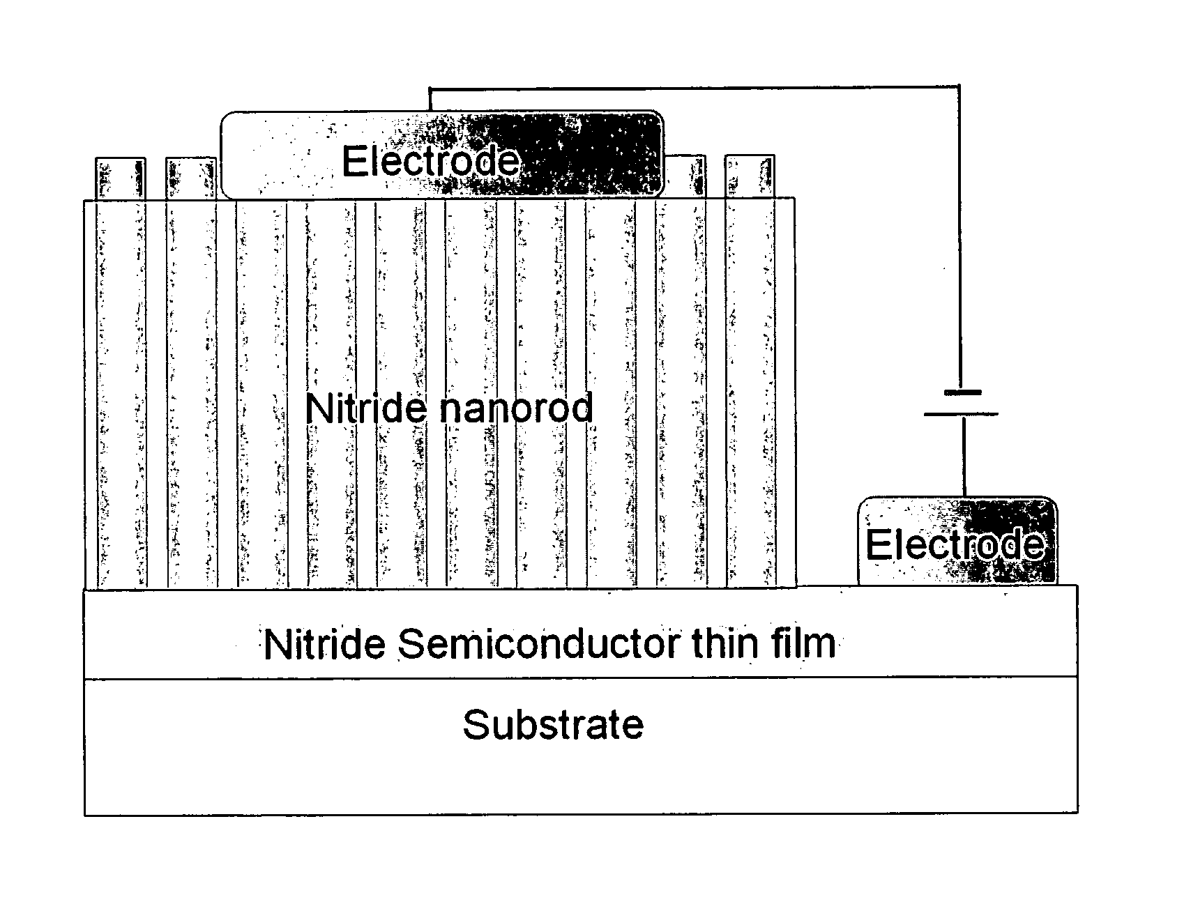
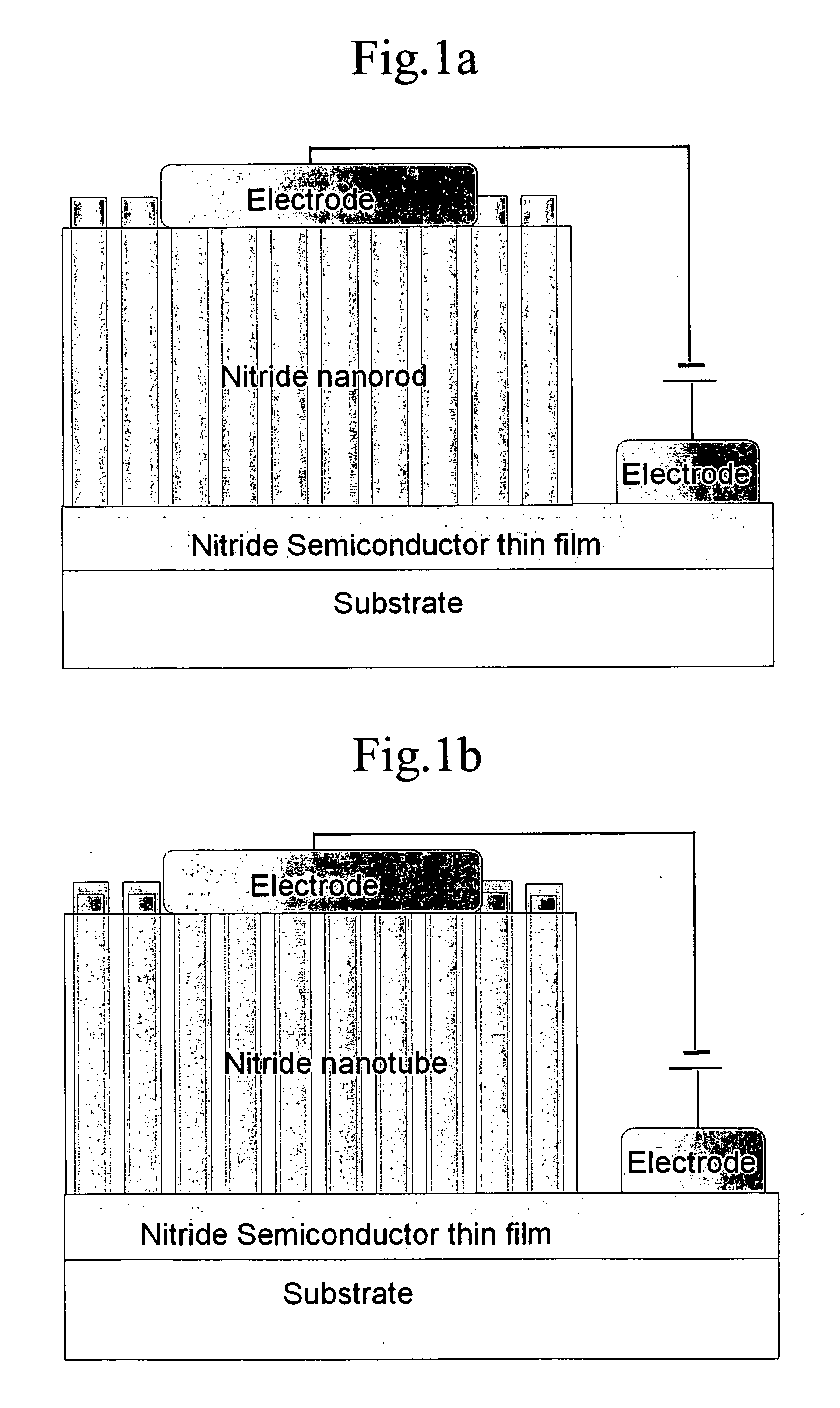
[0028] Then, n-type ZnO nanorods were vertically grown on the p-type GaN thin film thus obtained, by an MOCVD technique using diethylzinc (Zn(C2H5)2) and O2 with an argon (Ar) carrier gas. The reactor pressure and temperature were maintained in the ranges of 0.1 to 1,000 torr and 200 to 1,000° C., respectively, during one hour nanorod growth time.

[0029] After the completion of the growth of the n-ZnO nanorods on the p-GaN thin film, n-GaN was coated on the surface of the n-ZnO nanorods by injecting gaseous TMGa and NH3 into the reactor and reacting the vapors for 1 to 30 minutes, to obt...

example 2

Fabrication of a Light Emitting Device

[0033] Light emitting diodes were fabricated using the heterojunction structures prepared in Example 1 as follows.

[0034] First, the free space around the nanostructures, GaN / ZnO nanorods or GaN nanotubes, grown on a GaN thin film, was filled up by depositing an insulating material thereon, and then, the tip portion of the nanostructures was exposed by etching using a plasma. Subsequently, a Ti (10 nm) / Au (50 nm) top ohmic electrode was formed at the tip portion of the etched n-type nanostructures; and a Pt (10 nm) / Au (50 nm) bottom electrode, on the p-type GaN thin film, by a thermal or electron beam evaporation technique. The applied accelerating voltage and emission current were in the ranges of 4 to 20 kV and 40 to 400 mA, respectively, during the electrodes deposition, while keeping the reactor pressure at around 10−5 mmHg, and the substrate temperature at room temperature.

[0035] The cross-sectional morphology of the top electrode-formed ...


PUM


Abstract

A heterojunction structure composed of a nitride semiconductor thin film and nanostructures epitaxially grown thereon exhibits high luminescence efficiency property due to facilitated tunneling of electrons through the nano-sized junction, and thus can be advantageously used in light emitting devices.

Description

FIELD OF THE INVENTION [0001] The present invention relates to a novel heterojunction structure comprising a nitride semiconductor film and a nanostructure epitaxially grown thereon, which provides nano-devices having improved luminescence properties. BACKGROUND OF THE INVENTION [0002] The Gallium nitride (GaN)-based blue light emitting diode (LED) developed by Nichia Chemical Co., Ltd. in 1992 uses a GaN p-n thin film junction to provide blue and green LED devices, and in 1997, a short wavelength (404 nm) blue LED having a life span of about 10,000 hours at room temperature has been developed using a nitride semiconductor. [0003] Such light emitting devices, however, comprise a gallium nitride in the form of a thin film deposited on a sapphire substrate which requires a high manufacturing cost and gives a relatively low luminescence efficiency. SUMMARY OF THE INVENTION [0004] Accordingly, it is an object of the present invention to provide a novel nitride-based structure which can ...

Claims


Application Information

Patent Timeline
IPC IPC(8): H01L29/06H01L29/20H01L31/072H01L33/08H01L33/24
CPCB82Y10/00B82Y20/00H01L29/0665H01L29/0673H01L33/24H01L29/2003H01L33/08H01L33/18H01L29/0676
Inventor YI, GYU CHULAN, SUNG-JIN
Owner POSTECH ACAD IND FOUND
Why Eureka
Try Eureka