
Precursors for depositing silicon-containing films and processes thereof

a technology of silicon-containing films and precursors, which is applied in the direction of coatings, chemical vapor deposition coatings, metallic material coating processes, etc., can solve the problems of carbon contamination in the films, difficult control of the deposition of clean silicon nitride, and toxic compressed gas

Inactive Publication Date: 2005-08-18
VERSUM MATERIALS US LLC
View PDF10 Cites 104 Cited by
  • Summary
  • Abstract
  • Description
  • Claims
  • Application Information

AI Technical Summary

Benefits of technology

[0011] The present invention satisfies some, if not all, of the needs of the art by providing an inorganic precursor for the chemical vapor deposition of a silicon-containing film and a method, silicon-containing film, and reaction mixture comprising same. In one aspect of the present invention, there is provided a process for forming a silicon-containing film comprising: introducing a substrate and gaseous reagents comprising an iodosilane precursor having three or less iodine atoms bound to the silicon atom and at least

Problems solved by technology

Further, dichlorosilane is a pyrophoric, toxic compressed gas.
230-234, report deposition of silicon nitride using silane and ammonia by LPCVD at temperatures ranging from 250 to 400° C. Silane, however, is a pyrophoric gas and is difficult to control for the deposition of clean silicon nitride due to partial gas phase reaction.
Further, precursors that contain direct Si—C carbon bonds such as diethylsilane may cause carbon contamination in the films.
This temperature may still be too high for depositions on circuits with metallization and on many Group III-V and II-VI devices.
In addition, the precursor has a high activation energy that makes the process very temperature sensitive.

Method used


Image

  • Precursors for depositing silicon-containing films and processes thereof
  • Precursors for depositing silicon-containing films and processes thereof

Examples


examples

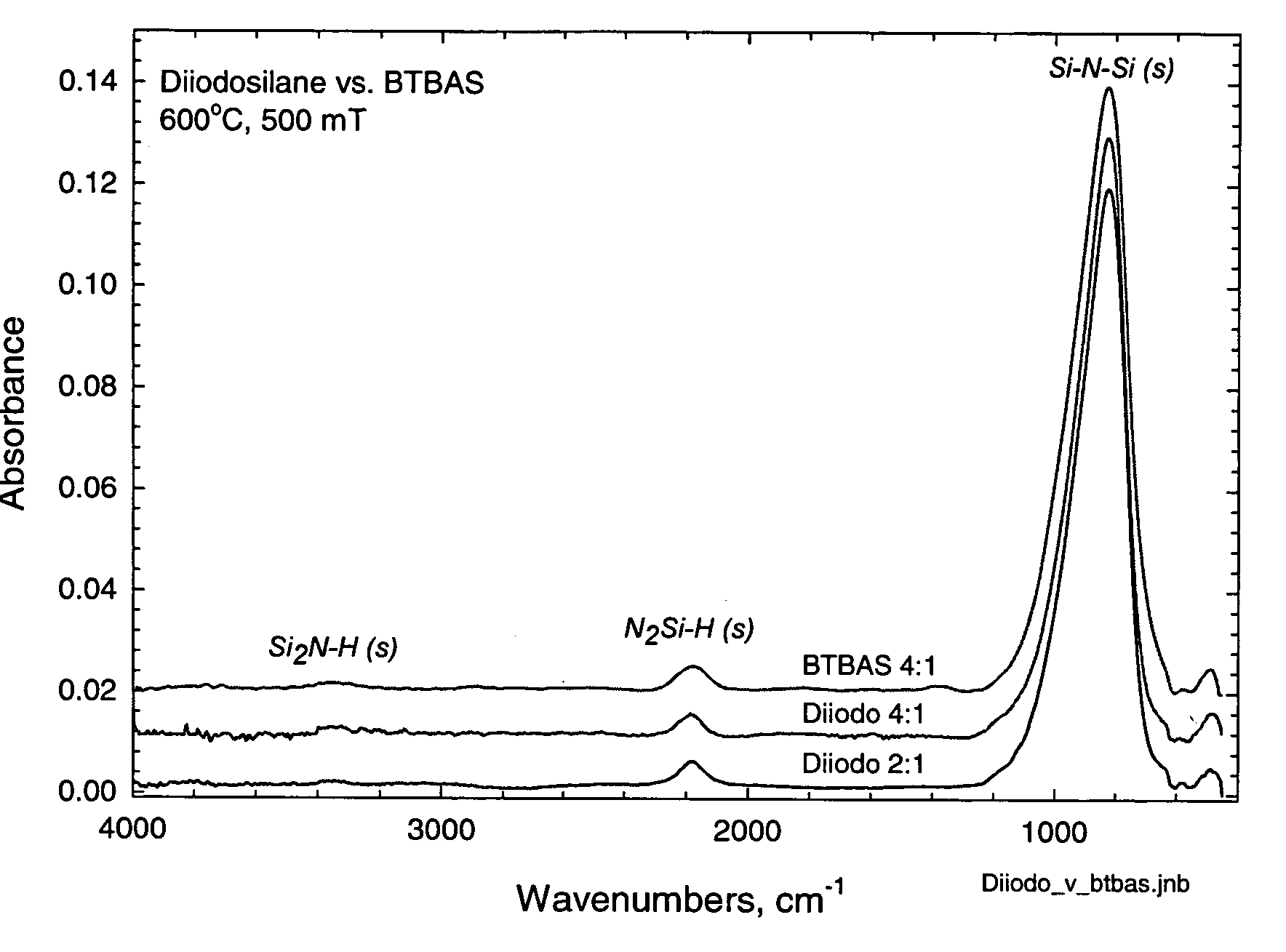
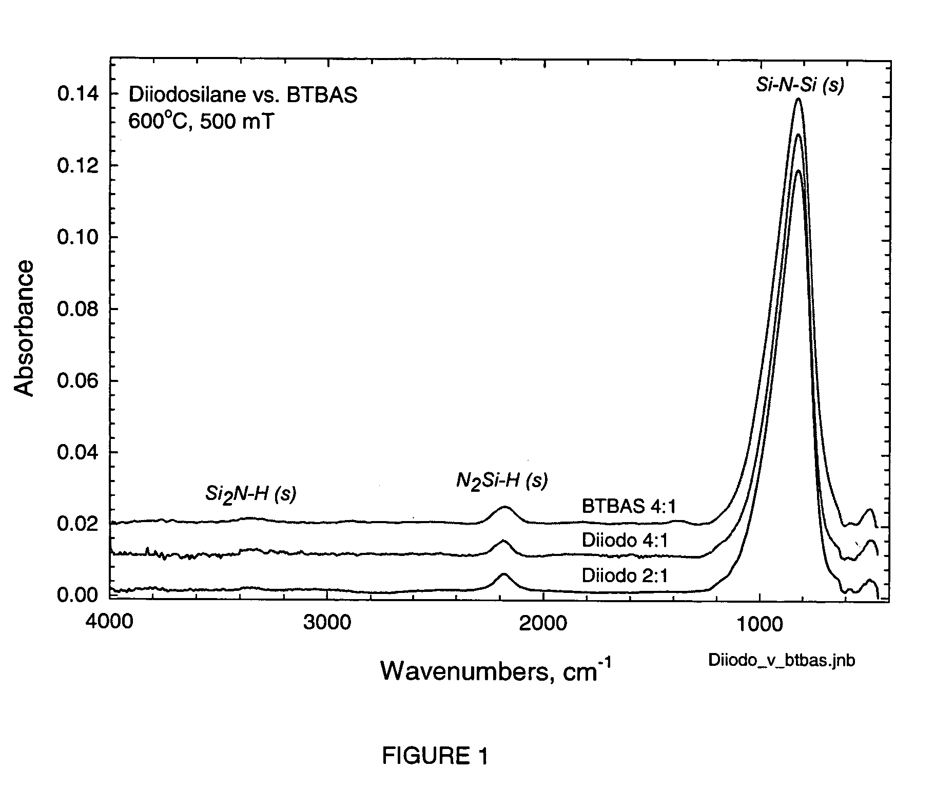
[0034] Silicon nitride films were formed onto silicon wafer substrates using diiodosilane as a precursor. The diiodosilane was purified by vacuum distillation and packaged within an inert atmosphere. Prior to use, the reagent was degassed through a series of freeze and thaw cycles under vacuum. For the depositions, the temperature of the iodosilane precursor was adjusted to provide a chemical vapor pressure of at least 10 Torr (1.33 kPa).

[0035] The films were formed in a horizontal flow isothermal reactor with a vacuum system consisting of a rotary vane pump / roots blower combination and various traps. The reactor pressure was controlled by a capacitance manometer feedback to a throttle valve controller. Reactor loading consisted of eighty 100 mm diameter silicon wafers at 9 mm spacing in standard diffusion boats. The boats were positioned on a sled, so that the wafers centers were slightly above the center of the reaction tube. This produced a uniform conductance around the wafer p...


PUM

PropertyMeasurementUnit
Temperatureaaaaaaaaaa

Abstract

Inorganic precursors, namely iodosilane precursors, for the low temperature, low pressure deposition of silicon-containing films is provided therein. In one aspect, there is provided a process for forming a silicon-containing film process comprising: introducing a substrate and gaseous reagents comprising an iodosilane precursor having three or less iodine atoms bound to the silicon atom and at least one reagent selected from an oxygen-containing reactive gas, a nitrogen-containing reactive gas, a hydrogen-containing reactive gas and mixtures thereof into a reaction chamber; heating the reaction chamber to one or more temperatures ranging from 200° C. to 900° C. to form the silicon containing film on the substrate, provided that if the iodosilane precursor has three iodine atoms bound to the silicon atom then the heating step is conducted at one or more pressures less than 600 Torr.

Description

BACKGROUND OF THE INVENTION [0001] In the fabrication of semiconductor devices, one or more thin layers of chemically inert, silicon containing dielectric films such as silicon nitride (Si3N4), silicon oxynitride, and silicon oxide may be needed. Silicon-containing dielectric films can be used on semiconductor devices as, for example, diffusion barriers, gate insulators for trench isolation, and capacitor dielectrics. These films may function, for example, as diffusion masks, oxidation barriers, intermetallic dielectric material with high dielectric breakdown voltages and passivation layers. For example, silicon-containing films, such as silicon nitride films, may be used as sidewall spacers in MOS devices and, with oxides, such as silicon oxynitride films, gate dielectrics for Groups IV and II-V transistors. Many other applications of silicon-containing dielectric films in the fabrication of semiconductor devices are reported elsewhere, see, i.e., Semiconductor and Process technolo...

Claims


Application Information

Patent Timeline
IPC IPC(8): C23C16/24C23C16/34C23C16/40C23C16/48H01L21/31H01L21/314H01L21/316H01L21/318H01L21/469
CPCC23C16/24C23C16/345C23C16/401C23C16/402H01L21/3185H01L21/3145H01L21/31608H01L21/31612H01L21/3144H01L21/02123H01L21/02205H01L21/02271
Inventor HOCHBERG, ARTHUR KENNETHCUTHILL, KIRK SCOTTDEIS, THOMAS ALANDEIS, LISA A.LAGENDIJK, ANDRE
Owner VERSUM MATERIALS US LLC
Learn More