Film bulk acoustic wave resonator
- Summary
- Abstract
- Description
- Claims
- Application Information
AI Technical Summary
Benefits of technology
Problems solved by technology
Method used
Image
Examples
example 1
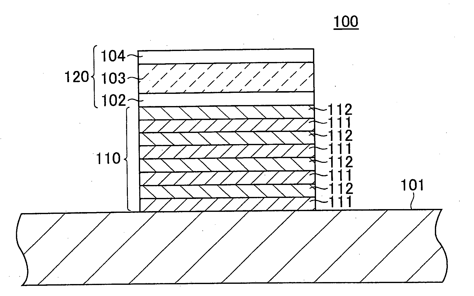
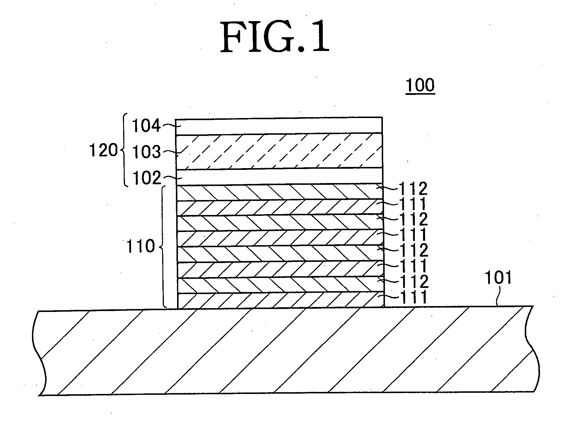
[0053] In Example 1, a number of film bulk acoustic wave resonators having the structure of the film bulk acoustic wave resonator 100 shown in FIG. 1 were fabricated by the following method.
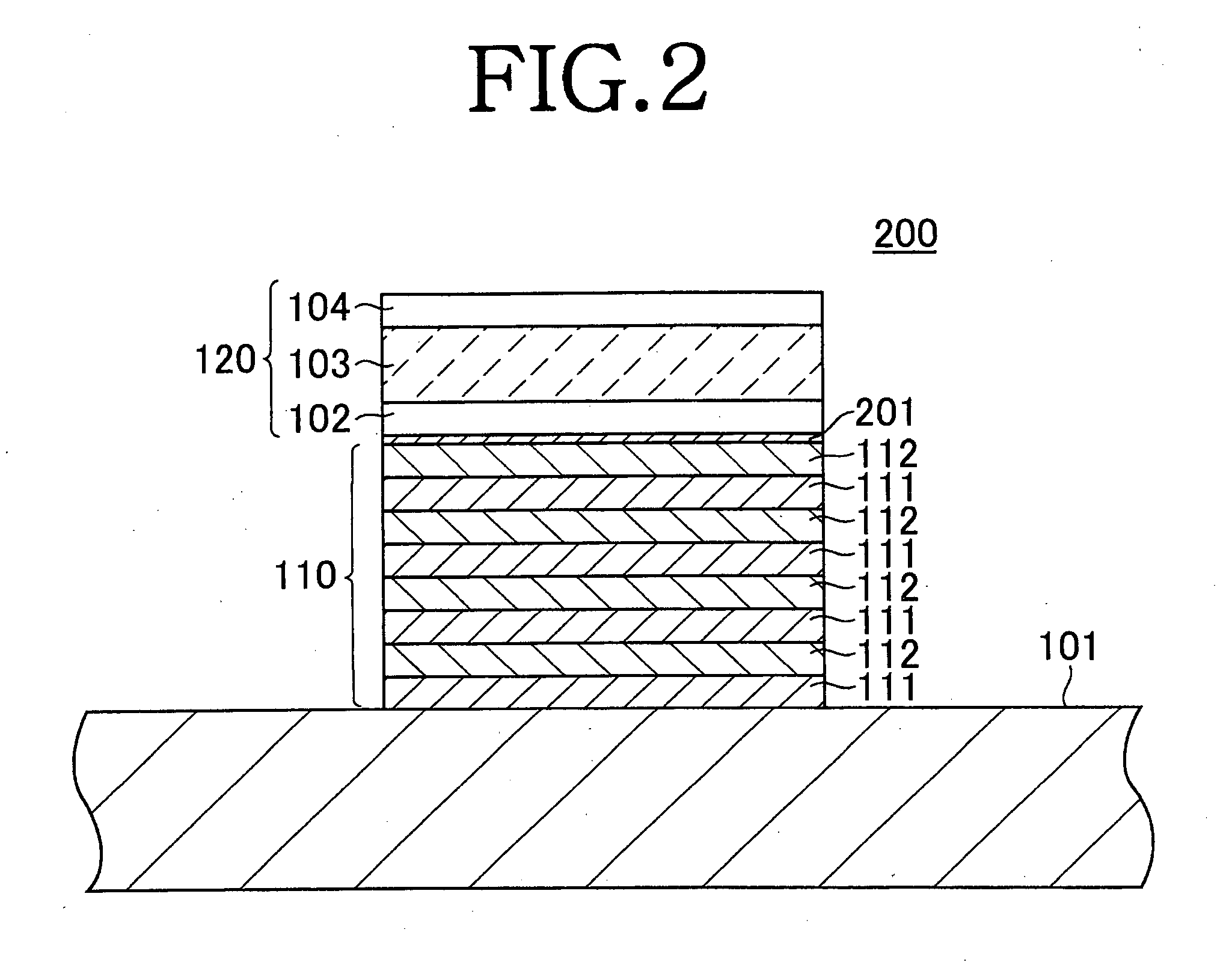
[0054] First, a Si (100) substrate 101 composed of mirror-polished Si single crystal and having a thickness of 250 μm and a resistivity of 1000 Ω·cm was prepared and washed. Next, the acoustic multilayer 110 was formed by repeating four cycles of a process in which a first reflective film 111 made of 1.5 μm thick AlN film formed by RF magnetron sputtering and a second reflective film 112 made of an 0.8 μm thick SiO2 film formed by RF magnetron sputtering were alternately overlaid in this order.
[0055] The first reflective film 111 was formed by sputtering, using aluminum (Al) as the target and an 80:20 mixture of argon (Ar) and nitrogen (N2) as the sputter gas. The chamber pressure was set at 0.5 Pa and the sputter temperature at 80° C.
[0056] The second reflective film 112 was formed by sputter...
example 2
[0062] The film bulk acoustic wave resonator of Example 2 was formed in the same way as in Example 1, except that the first reflective film 111 was formed using a 50:50 mixture of argon (Ar) and nitrogen (N2).
[0063] Measurement of the X-ray rocking curve of the aluminum nitride (AlN) first reflective film 111 of the film bulk acoustic wave resonator of Example 2 thus fabricated confirmed a strong peak in the (0001) plane; the rocking curve FWHM was approximately 10 degrees.
[0064] Next, the measuring instrument was connected to the film bulk acoustic wave resonator of Example 2 to measure the actual resonance characteristics. The measurement results are shown in FIG. 4.
[0065] As shown by FIG. 4, there were very few spurious readings caused by reflections from the substrate 101 of the film bulk acoustic wave resonator of Example 2. However, the impedance ratio was lower than in the case of the film bulk acoustic wave resonator of Example 1, which might be due to the different cryst...
PUM
 Abstract
Description
Claims
Application Information


