Compact inductor with stacked via magnetic cores for integrated circuits

Inactive Publication Date: 2005-09-01
ILLINOIS INSTITUTE OF TECHNOLOGY
View PDF18 Cites 80 Cited by
  • Summary
  • Abstract
  • Description
  • Claims
  • Application Information

AI Technical Summary

Benefits of technology

[0005] In response to the shortcomings of the prior art discussed above, the present invention provides for an on-chip or IC inductor which is compact enough to fit on a core circuit IC and has a magnetically permeable core which can be made with processes compatible with standard IC fabrication, thereby allowing a reduction in size from comparably performing inductors and providing economical fabrication costs, while achieving very high inductance and Q-factor values. In IC technology, the conducting plug used to connect silicon (Si) and the first metal layer is called a “contact” and a conductor plug used to connect other higher level metal layers is called a “via.” The present invention provides an

Problems solved by technology

Current micro-inductors are very large in size and feature low quality factors (Q-factor) due to magnetic losses.
Further, the techniques for manufacturing micro-inductors are not compatible with standard IC fabrication techniques, resulting in greater time and expense to obtain the on-chip inductors.
However, these microelectromechanical-based techniques are not truly compatible with CMOS (complementary metal oxide semiconductor) IC fabrication techniques because many add-on steps outside of traditional wafer fabrication are required in MEMS technology and therefore will add substantial costs to IC fabrication even if successful integration of MEMS and CMOS fabric

Method used


Image

  • Compact inductor with stacked via magnetic cores for integrated circuits
  • Compact inductor with stacked via magnetic cores for integrated circuits
  • Compact inductor with stacked via magnetic cores for integrated circuits

Examples


Embodiment Construction

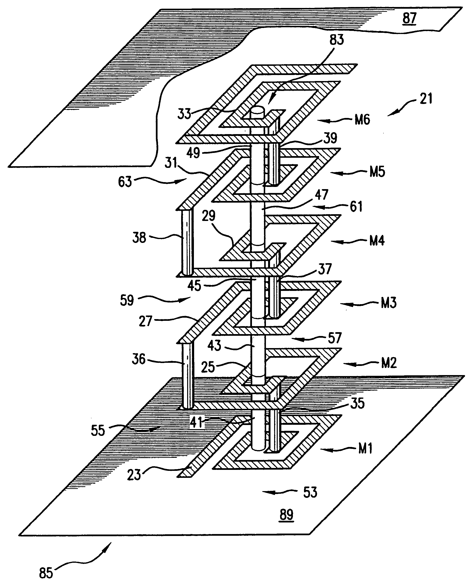
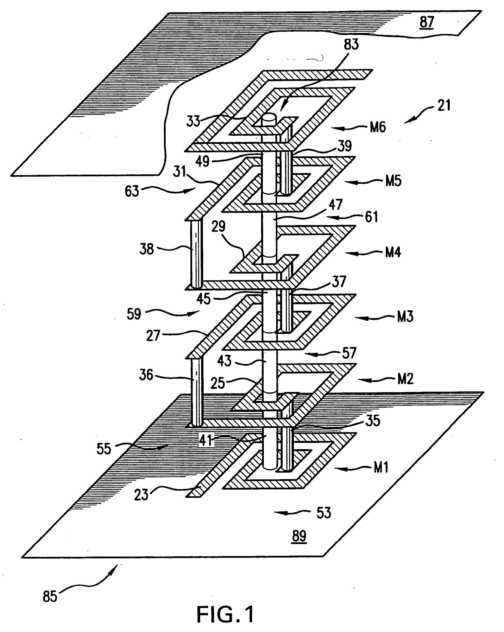
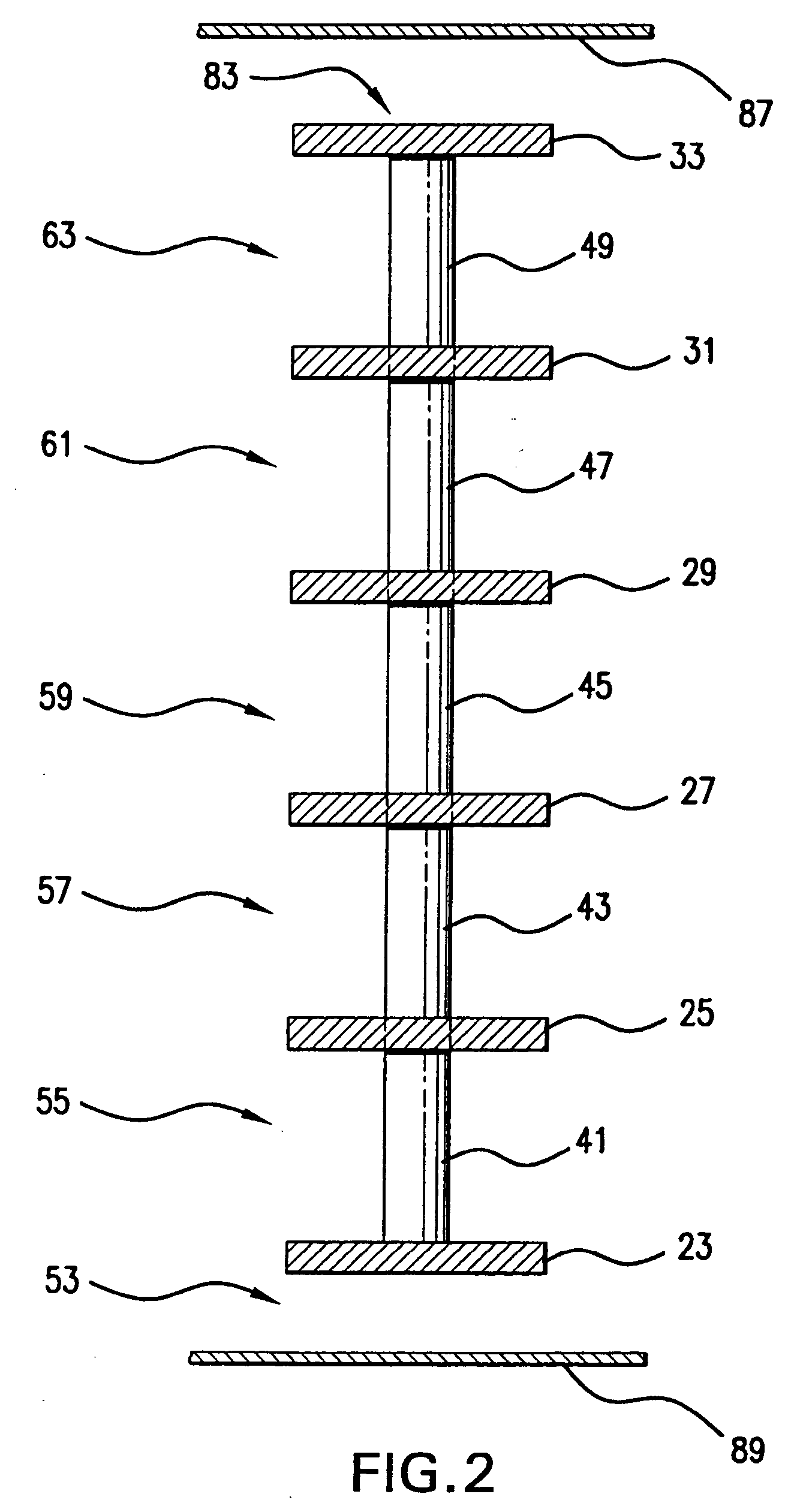
[0013]FIGS. 1-3 illustrate the layout of a stacked spiral IC inductor 21. FIGS. 1 and 2 show the inductor structure with the surrounding material removed. FIG. 3 shows surrounding structure and the base layers. In FIGS. 1-3 the inductor 21 is shown with a single stacked via bar magnetic core 83 according to one aspect of the present invention using a typical six-metal IC technology, where there are six metal layers M1-M6, one contact via plug level 53 and five via plug levels 55, 57, 59, 61, and 63. Six planar spiral coils 23, 25, 27, 29, 31, 33 formed from the six metal deposition layers are shown. The electrical connectors 35, 37, 39 connect the spiral coils 23-25, 27-29 and 31-33 at the inside of the coils; and electrical connectors 36, 38 connect coils 25-27 and 29-31 on the outside of the coils. FIG. 3 shows the IC inductor 21 as attached to a core circuit 85 on the same IC.

[0014] It will be understood by the person of skill in the art that the illustrated embodiment is for ex...


PUM


Abstract

An on-chip inductor device for Integrated Circuits utilizes coils on a plurality of metal layers of the IC with electrical connectors between the coils and a magnetic core for the inductor of stacked vias running between the coils. The magnetic core is made from a series of stacked vias which are deposited between each metal layer of the IC having a coil. The magnetic core desirably includes an array of magnetic bars comprising the magnetic core. The via material of the magnetic core may be both magnetic and electrically conductive. The magnetic and electrically conductive via material may also be used for the planar coil electrical connectors or other electrically conductive parts of the IC, or both, thereby lessening fabrication steps. Films of magnetic material may be formed at the ends of the inductor to provide a closed magnetic circuit for the inductor. A high Q factor inductor of small (e.g., transistor) size is thus obtained. The materials and processes which enable the on-chip inductor device are compatible with ordinary IC fabrication methods.

Description

BACKGROUND OF THE INVENTION [0001] High performance on-chip inductors and transformers (hereafter sometimes referred as “inductors” or “micro-inductors” for simplicity) are highly desirable in mixed-signal / RF IC (radio frequency integrated circuit) design for increased miniaturization and performance and low power consumption for RF equipment. Past research has resulted in substantial advances in making micro-inductors. Designs ranging from simple stacked planar spiral inductors to complex MEMS (microelectromechanical system) inductors are currently known. However, further improvements over known designs are still desired. Current micro-inductors are very large in size and feature low quality factors (Q-factor) due to magnetic losses. Further, the techniques for manufacturing micro-inductors are not compatible with standard IC fabrication techniques, resulting in greater time and expense to obtain the on-chip inductors. [0002] Complex MEMS techniques have been proposed to make micro...

Claims


Application Information

Patent Timeline
IPC IPC(8): H01F5/00H01F17/00H01F41/04H01L23/522
CPCH01F17/0013H01F41/046H01L28/10H01F2017/0066H01L23/5227H01F2017/002H01L2924/0002H01L2924/00
Inventor WANG, ALBERT Z.H.
Owner ILLINOIS INSTITUTE OF TECHNOLOGY
Why Eureka
Try Eureka