Bonded substrate, surface acoustic wave chip, and surface acoustic wave device

a surface acoustic wave and substrate technology, applied in the direction of device material selection, piezoelectric/electrostrictive device material selection, generator/motor, etc., can solve the problems of piezoelectric materials, lt and ln have inferior temperature stability, and the temperature of the passband depends on the temperature, so as to achieve excellent temperature stability, small distortion, and sufficient bonding strength

Active Publication Date: 2005-09-08
TAIYO YUDEN KK
View PDF3 Cites 29 Cited by
  • Summary
  • Abstract
  • Description
  • Claims
  • Application Information

AI Technical Summary

Benefits of technology

[0012] A more specific object of the present invention is to provide the SAW chip having a bonded su

Problems solved by technology

However, LT and LN have a drawback of inferior temperature stability.
The SAW chip made with the above-mentioned piezoelectric materials has a problem in that the passband depends on temperature.
In contrast, a quartz crystal, which is also a piezoelectric material of the SAW chip, is superior in the temperature stability, but has a drawback of the small electromechanical coupling coefficient.
The piezoelectric material having a large electromechanical coupl

Method used


Image

  • Bonded substrate, surface acoustic wave chip, and surface acoustic wave device
  • Bonded substrate, surface acoustic wave chip, and surface acoustic wave device
  • Bonded substrate, surface acoustic wave chip, and surface acoustic wave device

Examples


Embodiment Construction

[0023] A description will now be given, with reference to the accompanying drawings, of embodiments of the present invention.

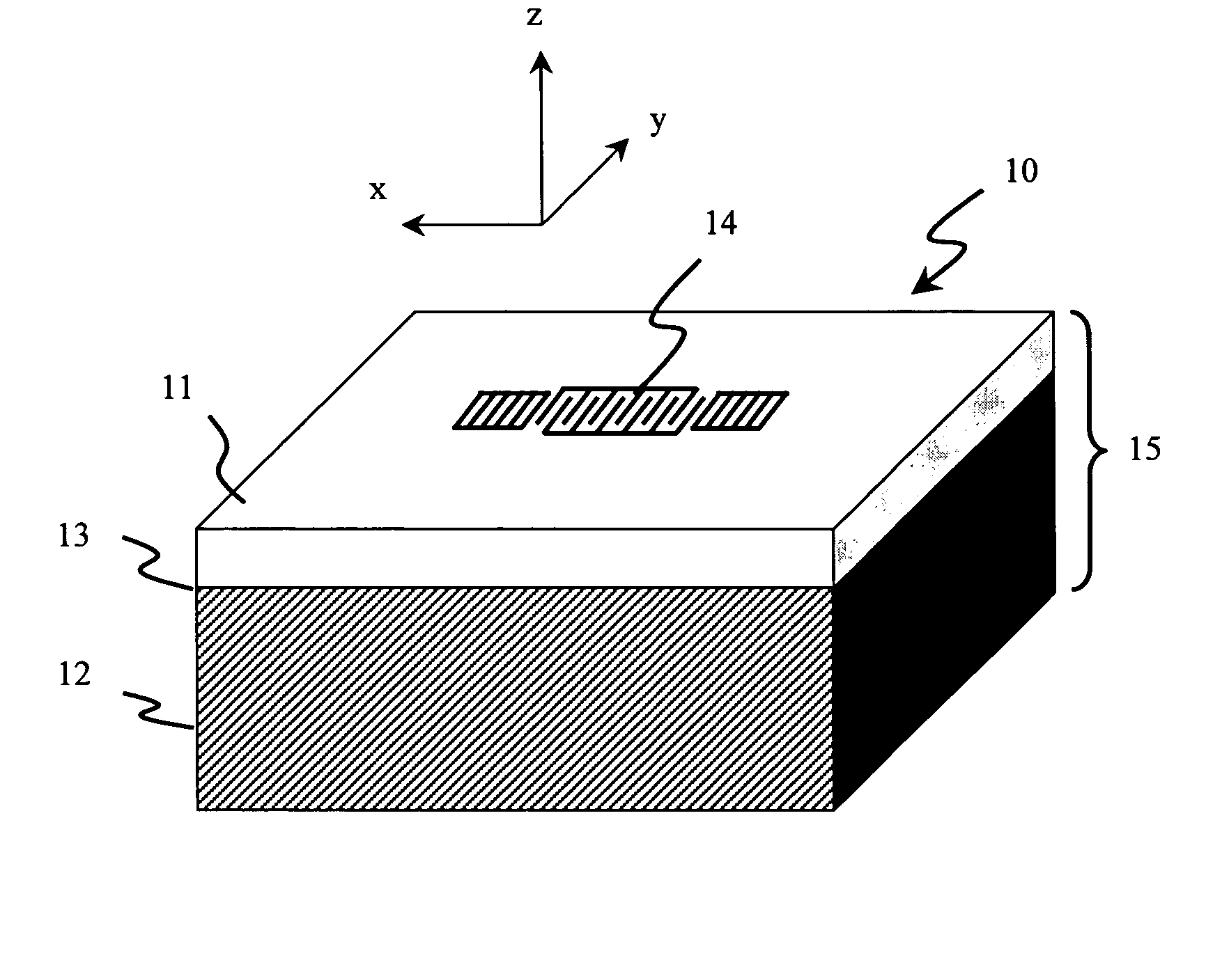
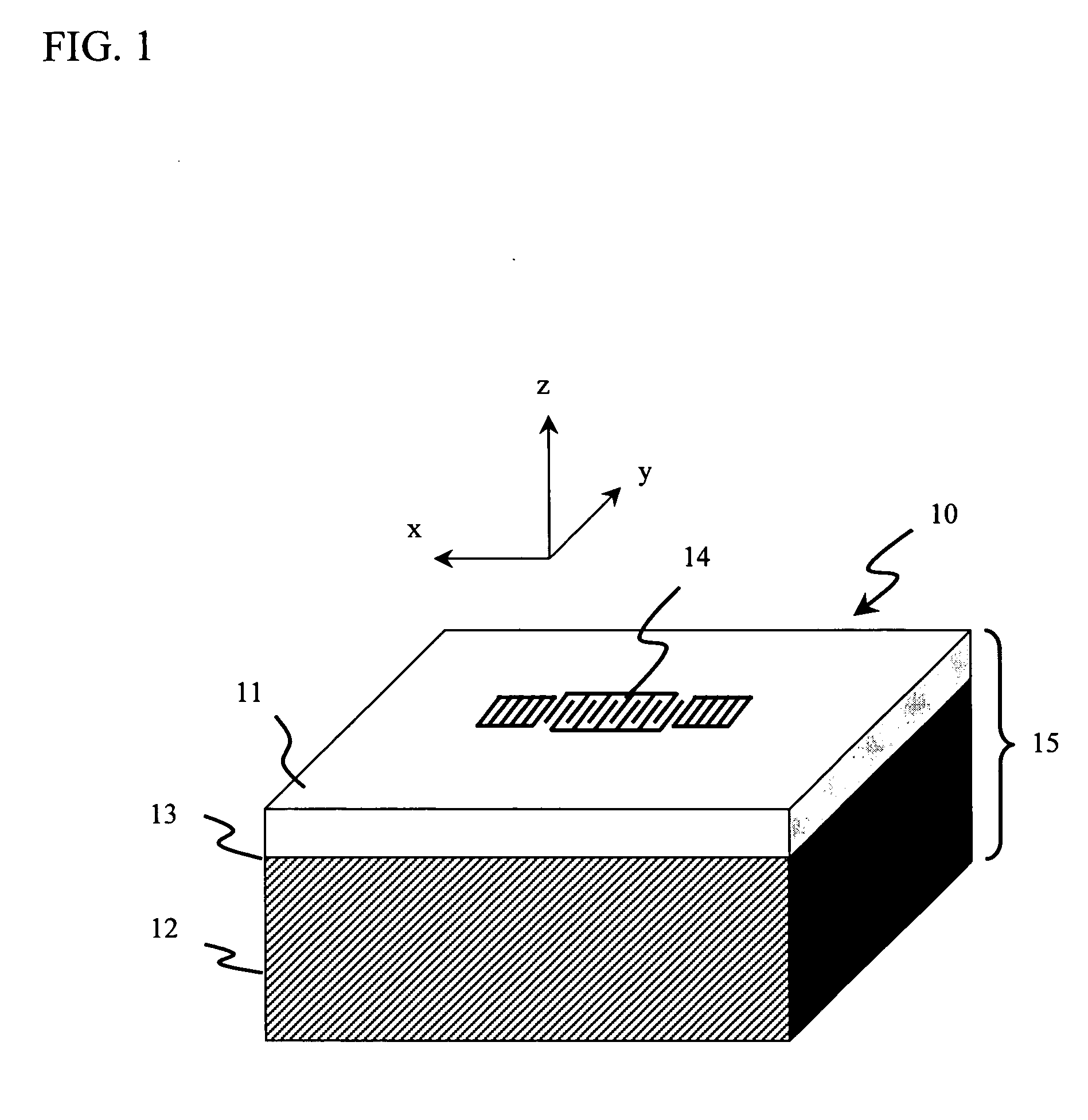
[0024]FIG. 1 is a perspective view of a SAW chip made with a bonded substrate in accordance with the present invention. A SAW chip 10 includes a bonded substrate 15. The bonded substrate 15 includes a piezoelectric substrate 11, a supporting substrate 12, and a bonded interface 13 in an amorphous state. The piezoelectric substrate 11 and the supporting substrate 12 are bonded through the bonded interface 13. A SAW resonator 14 is provided on a main surface of the piezoelectric substrate 11 so that the SAW propagates in the X direction.

[0025] The piezoelectric substrate 11 employs a single-crystalline LT substrate of 42-degree rotated Y-cut around the X-axis of a propagation direction (42° Y-cut X-propagation LT substrate). The single-crystalline LT substrate has a thickness of 40 μm. The linear expansion coefficient of the SAW propagation direction X of the ...


PUM


Abstract

A bonded substrate includes a lithium tantalate substrate and a sapphire substrate to which the lithium tantalate substrate is bonded, a bonded interface of the lithium tantalate and the sapphire substrate includes a bonded region in an amorphous state having a thickness of 0.3 nm to 2.5 nm. The bonded region in the amorphous state is formed by activating at least one of the lithium tantalate substrate and the sapphire substrate in the bonded interface with neutralized atom beams, ion beams or plasma of inert gas or oxygen. It is possible to bond the piezoelectric substrate to the supporting substrate having different lattice constants without the high-temperature thermal treatment and realize the bonded substrate having an excellent bonding strength and being less warped.

Description

BACKGROUND OF THE INVENTION [0001] 1. Field of the Invention [0002] This invention generally relates to a bonded substrate and a surface acoustic wave chip, and more particularly, to a substrate in which a lithium tantalate substrate and a sapphire substrate are bonded and a surface acoustic wave chip equipped with the bonded substrate. [0003] 2. Description of the Related Art [0004] A surface acoustic wave (hereinafter referred to as SAW) device is produced with a piezoelectric substrate having comb-like electrodes thereon. A high-frequency power is applied to one comb-like electrode to generate surface acoustic waves, and another comb-like electrode converts the surface acoustic waves into high-frequency signals. [0005] The SAW device has a wavelength smaller than that of an electromagnetic wave by 10−5. Therefore, the SAW device can be downsized. The SAW device has a high efficiency in propagation because of a low loss. Additionally, the technique on semiconductor manufacturing p...

Claims


Application Information

Patent Timeline
IPC IPC(8): H01L41/18H01L41/09H01L41/22H01L41/23H01L41/312H03H9/02H03H9/25
CPCH03H9/02574H03H9/02559H10N30/072H03H9/25H03H9/145H03H9/64
Inventor MIURA, MICHIOUEDA, MASANORIAIKAWA, SHUNICHIUEMURA, TORUWADA, KUNIHISAMISHIMA, NAOYUKI
Owner TAIYO YUDEN KK
Why Eureka
Try Eureka