Current-mode direct conversion receiver

a current-mode direct conversion and receiver technology, applied in the direction of transmission noise suppression, transmission, electric equipment, etc., can solve the problems of limiting the ease of use of rf receivers, non-ideal effects, and inability to operate, so as to minimize the input impedance (and voltage perturbations), minimize the input signal self-mixing, and minimize noise

Active Publication Date: 2005-09-08
MICROCHIP TECH INC
View PDF7 Cites 46 Cited by
  • Summary
  • Abstract
  • Description
  • Claims
  • Application Information

AI Technical Summary

Benefits of technology

[0009] In one embodiment, the current-mode direct conversion receiver includes an input transconductance stage that converts the input RF signal into a current mode signal. The input transconductor replaces the traditional voltage-mode low noise amplifier (LNA) of conventional RF receivers. A high impedance output of the input transconductor may be connected to a very low input impedance current cascode stage. The current cascode stage may feed into a down conversion mixer stage, which may generate quadrature current outputs. In one embodiment, the current cascode stage is constructed with common source transistors in a feedback loop and may operate to minimize the input impedance (and voltage perturbations) seen at the current cascode inputs. Overall, the current cascode stage may operate to isolate the RF input from any voltage changes seen due to the down conversion mixer stage, in order to minimize self-mixing with the input signal.

Problems solved by technology

Often some additional gain is also used before down converting the input RF signal as the mixing process typically adds noise to the baseband signal.
A large supply voltage limits the ability of RF receivers to operate from portable supply voltages, for example a battery, which limits their ease of use.
Disadvantages of direct conversion receiv

Method used


Image

  • Current-mode direct conversion receiver
  • Current-mode direct conversion receiver
  • Current-mode direct conversion receiver

Examples


Embodiment Construction

[0018] As used herein, when referencing a pulse of a signal, a “leading edge” of the pulse is a first edge of the pulse, resulting from the value of the signal changing from a default value, and a “trailing edge” is a second edge of the pulse, resulting from the value of the signal returning to the default value. A “data-valid window” for a signal represents a time period during which the signal may be considered a valid digital signal. A first signal is said to be “corresponding” to a second signal if the first signal was generated in response to the second signal. A first signal is said to “propagated based on” a second signal, when the second signal controls the propagation of the first signal. Similarly, a first module is said to “use” a clock signal to transfer data to a second module, when propagation of the data from the first module to the second module is controlled and / or triggered by the clock signal.

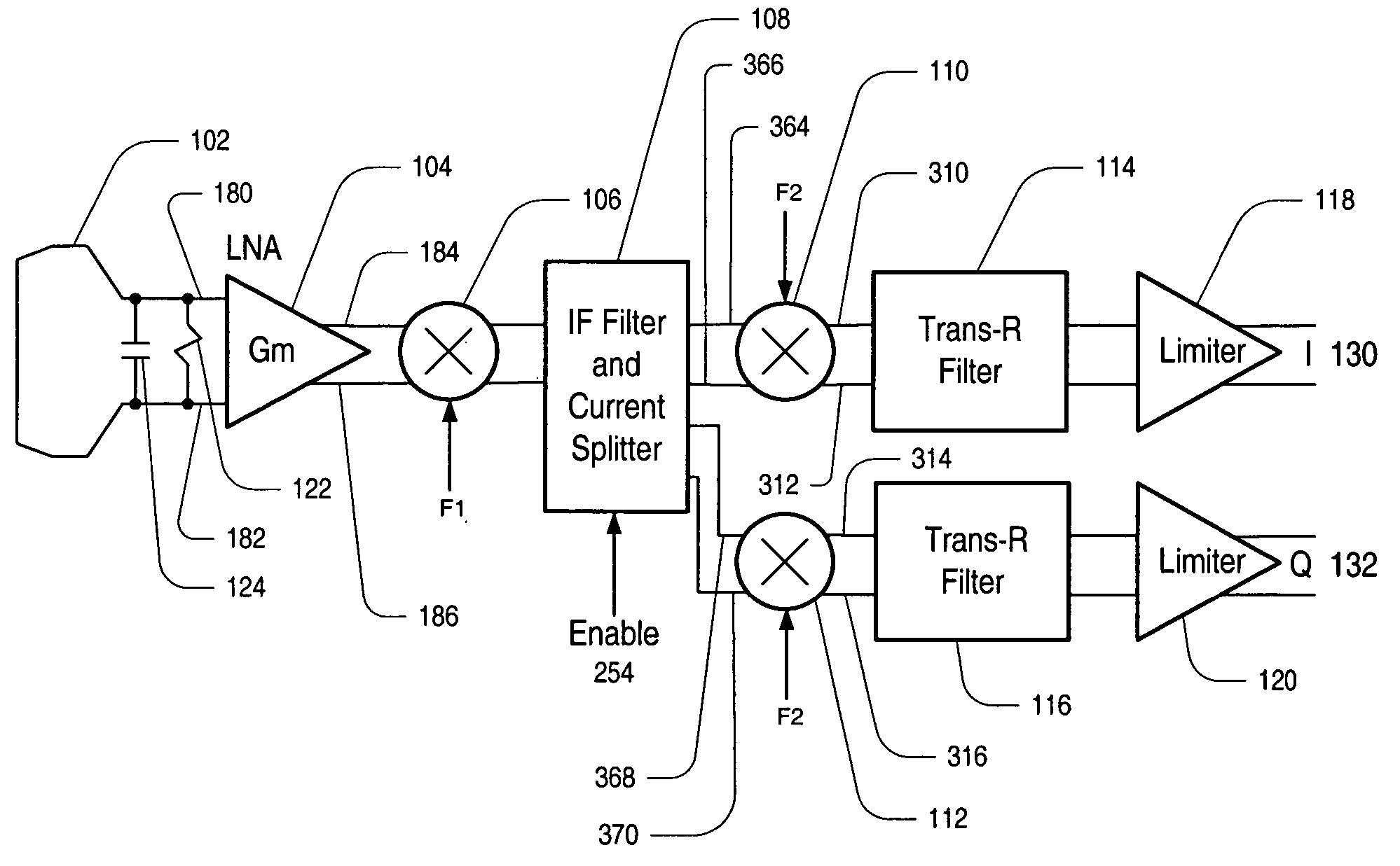
[0019]FIG. 1 illustrates a receiver architecture implemented in accorda...


PUM


Abstract

A current-mode direct conversion RF receiver is presented. In one set of embodiments the RF receiver comprises a simple transconductor input stage to create a current-mode modulated signal from a voltage-mode modulated signal. A downconversion mixer may be coupled to the transconductor input stage via a low impedance current cascode stage, and may operate to create a set of current-mode quadrature baseband signals from the current-mode modulated signal. The downconversion mixer may be implemented with a transistor-switching network, which may be driven by a phase locked loop (PLL) with quadrature outputs. The set of current-mode quadrature baseband signals may be converted back to the voltage domain by a transimpedance filter, which may perform channel selection for the receiver. The transimpedance filter may additionally include a low frequency zero to remove DC offsets. The receiver may be implemented using CMOS design technologies and operated with minimal self-mixing effects, minimal DC offset in the baseband signal, and utilizing low voltages.

Description

BACKGROUND OF THE INVENTION [0001] 1. Field of the Invention [0002] This invention relates generally to the field of wireless electronic equipment design and, more particularly, to radio frequency (RF) receiver design. [0003] 2. Description of the Related Art [0004] A traditional narrow band radio system's receiver portion is generally used for translating a modulated radio frequency (RF) carrier to a low frequency, or baseband, signal, which may then be demodulated to extract an original modulating signal. A primary function of an RF receiver is best described as a “down conversion”, or “mixing”, of an RF modulated carrier to a baseband signal, and a filtering of the down converted signal to remove any artifacts that may have arisen as part of the mixing process. Due to the image effects that may occur during the mixing process, performing down conversion may be handled in multiple stages where two or more down conversion stages may be applied in series. A traditional super-heterod...

Claims


Application Information

Patent Timeline
IPC IPC(8): H04B1/00H04B1/69H04B1/707H04B1/713
CPCH04B1/30
Inventor STOCKSTAD, TROY L.WORTEL, KLAASBRIONES, LUIS J.LOVELACE, DAVID
Owner MICROCHIP TECH INC
Why Eureka
Try Eureka