Electroplating solution, method for manufacturing multilayer printed circuit board using the same solution, and multilayer printed circuit board

Inactive Publication Date: 2005-09-29
IBIDEN CO LTD
View PDF19 Cites 24 Cited by
  • Summary
  • Abstract
  • Description
  • Claims
  • Application Information

AI Technical Summary

Benefits of technology

[0010] Further, a stack via structure (a structure in which a via-hole is formed immediate above another via-hole, reference to FIG. 1) is required as a structure of a multilayer-built-up printed circuit board to shorten the wiring distance in order to provide a printed circuit board wi

Problems solved by technology

As described above, in a multilayer-built-up printed circuit board, the upper face of the conductor circuit, especially the peripheral part of a via-hole, is not flat, so that in the case of forming an interlaminar resin insulating layer on the upper face of conductor circuit, the interlaminar resin insulating layer is sometimes waved to result in separation of the interlaminar resin insulating layer and crack formation and disconnection of the conductor circuit to be formed on the upper layer of the interlaminar resin insulating layer as well.
However, since an opening part for a via-hole in a multilayer-built-up printed circuit board manufactured by a conventional method as described above is not perfectly filled with a metal, it becomes difficult to form the stack via structure.

Method used


Image

  • Electroplating solution, method for manufacturing multilayer printed circuit board using the same solution, and multilayer printed circuit board
  • Electroplating solution, method for manufacturing multilayer printed circuit board using the same solution, and multilayer printed circuit board
  • Electroplating solution, method for manufacturing multilayer printed circuit board using the same solution, and multilayer printed circuit board

Examples


example 1

[0224] A. Preparation of a Resin Composite (an Adhesive for an Upper Layer)

[0225] (i) A mixture composition was produced by blending 35 parts by weight of a resin solution produced by dissolving 80 wt. % of a cresol novolak type epoxy resin acrylated in 25% (made by Nippon Kayaku Co., Ltd.: molecular weight 2,500) in diethylene glycol dimethyl ether (DMDG), 3.15 parts by weight of a photosensitive monomer (made by Toagosei Chemical Industry Co., Ltd.: Aronix M 315), 0.5 parts by weight of a defoaming agent (made by San Nopco Ltd.: S-65), and 3.6 parts by weight of N-methylpyrrolidone (NMP) in a container and mixing and stirring them.

[0226] (ii) Another mixture composition was produced by blending 12 parts by weight of polyether sulfone (PES), 7.2 parts by weight of an epoxy resin particle (made by Sanyo Chemical Industries, Ltd.: Polymerpol) with the average particle size of 1.0 μm and 3.09 parts by weight of the particle with the average particle size of 0.5 μm in another contain...

example 2

[0267] A. A Method for Manufacturing a Printed Circuit Board

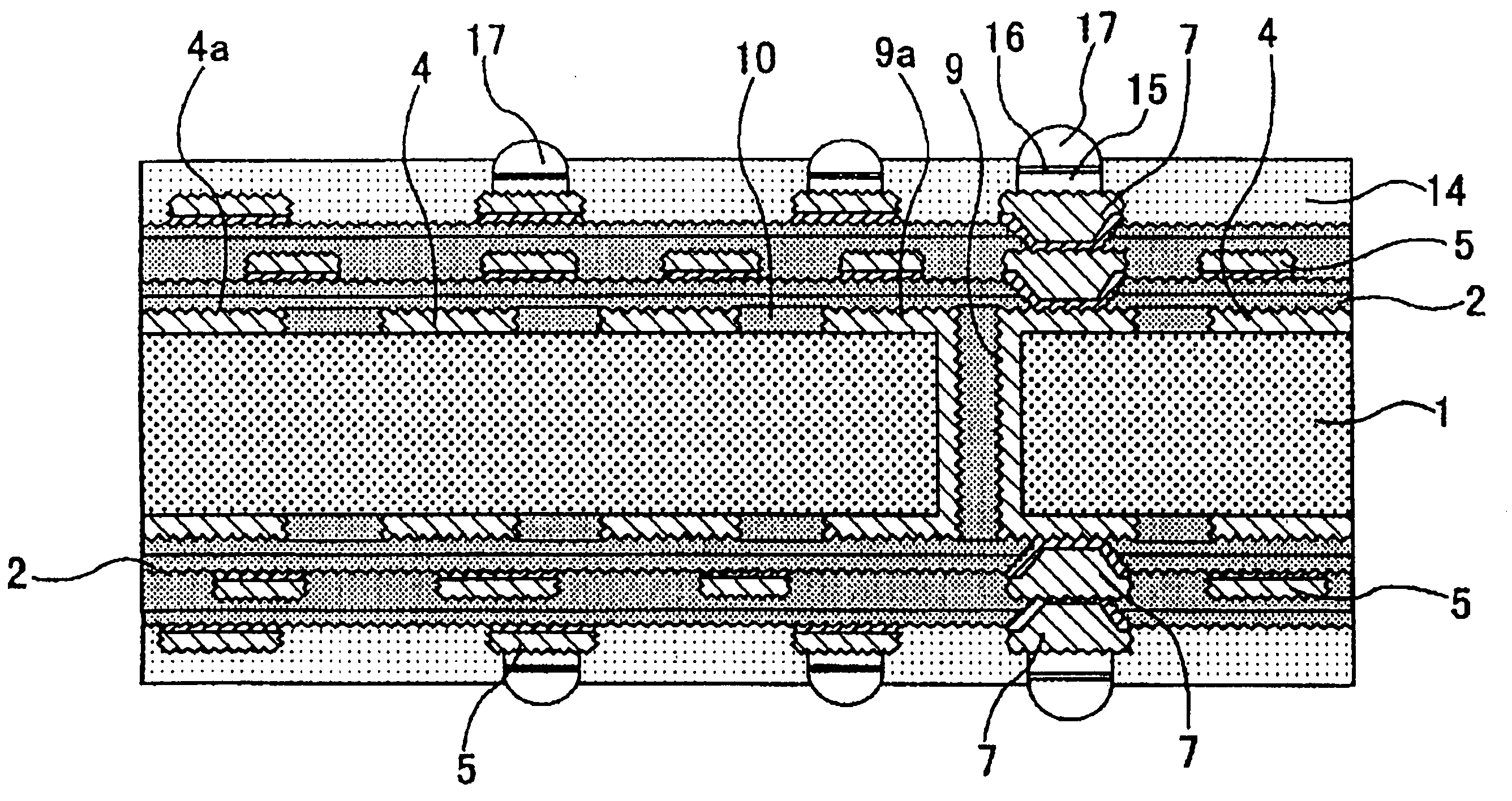
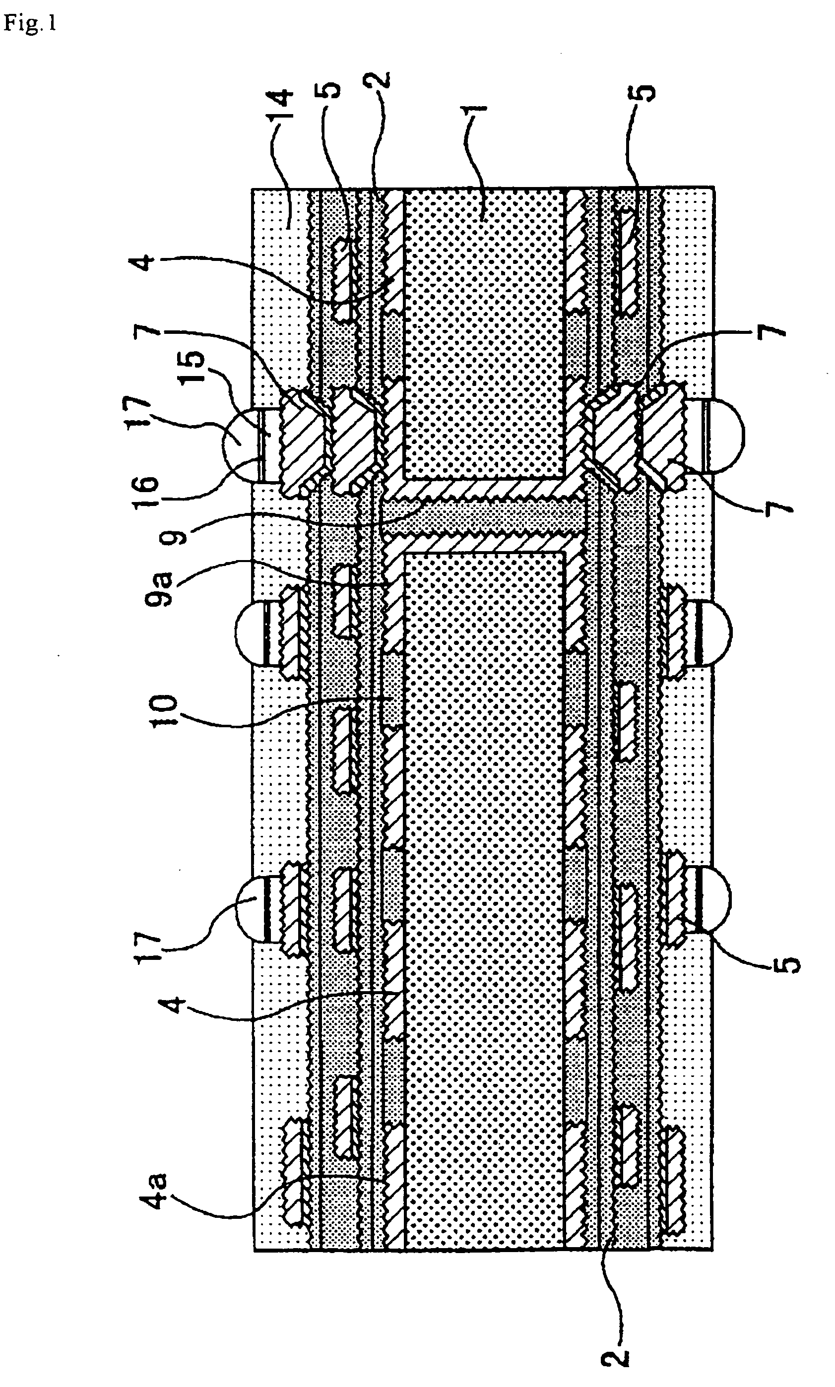
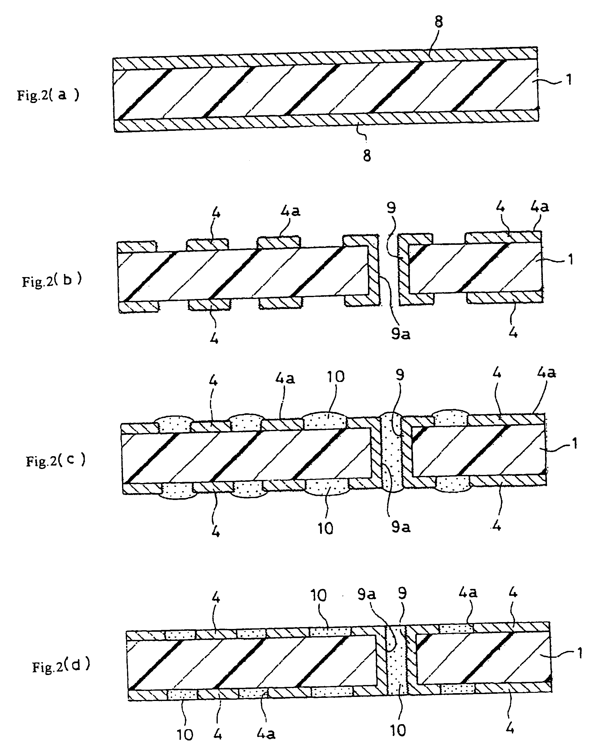
[0268] (1) A copper-laminated laminate plate composed of a substrate 1 which is made of a 0.8 mm-thick glass epoxy resin or BT (bismaleimide triazine) resin with a 18 μm-thick copper foil 8 laminated on both sides of the substrate 1 was used as a starting material (reference to FIG. 8(a)). At first, the copper-laminated laminate plate was drilled to form a through hole, subjected to electroless plating treatment and then etching treatment in a pattern to form an under-level conductor circuit 4 in both sides of the substrate 1 and a plated-through hole 9.

[0269] (2) After the resultant substrate in which the plated-through hole 9 and the under-level conductor circuits 4 are formed was washed with water and dried, the following etching solution was sprayed to both sides of the substrate to etch the under-level conductor circuits 4 and the land surface and the inner wall of the plated-through hole 9 and form roughened surface...

example 3

[0294] A. A Method for Manufacturing a Printed Circuit Board

[0295] (1) In the same manner as the processes (1) to (8) of the example 1, a substrate bearing conductor circuits 4 and resin insulating layers 2 was produced and after that, an electroless copper plating film 12 was formed in the same manner as the process (9) of the example 1 (reference FIG. 14(a) to FIG. 16 (a)).

[0296] (2) A photosensitive dry film sold on the market was stuck to the electrolytic copper plating film 12, a mask was put thereon, exposure was carried out at 100 mJ / cm2, and development treatment was carried out with an aqueous solution of 0.8% sodium carbonate to form a plating resist 23 with the thickness of 15 μm (reference FIG. 16(b)).

[0297] (3) Next, electroplating of the parts where no plating resist 23 was formed was carried in the following conditions to form an electroplating film 13 with the thickness of 7.5 μm (reference to FIG. 15(c)):

[0298] [The Aqueous Electroplating Solution]

CuSO4—5H2O210 ...


PUM

PropertyMeasurementUnit
Densityaaaaaaaaaa
Densityaaaaaaaaaa
Densityaaaaaaaaaa

Abstract

The objective of present invention is to provide an electroplating solution capable of forming the upper face of a via-hole and the upper face of a conductor circuit in the same layer in approximately the same plane at the time of manufacturing a multilayer printed circuit board. The electroplating solution of the present invention is characterized by containing 50 to 300 g / L of copper sulfate, 30 to 200 g / L of sulfuric acid, 25 to 90 mg / L of chlorine ion, and 1 to 1000 mg / L of an additive comprising at least a levelling agent and a brightener.

Description

CROSS REFERENCE TO RELATED APPLICATIONS [0001] This is a divisional of application Ser. No. 10 / 048,852 filed Apr. 11, 2002, which is a National Stage Application filed under §371 of PCT Application No. PCT / JP00 / 04418 filed Jul. 4, 2000; the above noted applications incorporated herein by reference.TECHNICAL FIELD [0002] The present invention relates to an electroplating solution to be employed for manufacturing a multilayer printed circuit board, a method for manufacturing a multilayer printed circuit board using the electroplating solution, and a multilayer printed circuit board. [0003] A multilayer printed circuit board so-called a multilayer-built-up wiring substrate is manufactured by a semi-additive method and the like and produced by building up a conductor circuit of copper and the like and an interlaminar resin insulating layer on a resin substrate, so-called a core, of approximately 0.5 to 1.5 mm thickness and reinforced with glass cloths and the like serially in alternate ...

Claims


Application Information

Patent Timeline
IPC IPC(8): C25D3/38H05K1/11H05K3/10H05K3/34H05K3/38H05K3/42H05K3/46
CPCC25D3/38H05K1/113H05K3/108H05K3/3457Y10T29/49155H05K3/423H05K3/4602H05K3/4661H05K2201/09563H05K3/388
Inventor EN, HONCHIN
Owner IBIDEN CO LTD
Why Eureka
Try Eureka