Dual-processor complex domain floating-point DSP system on chip

a floating-point dsp and complex domain technology, applied in the field of multi-processor systems, can solve problems such as limiting algorithm development and adaptation for these systems, prior art failing to recognize this opportunity, and suffering from a number of limitations

Active Publication Date: 2005-09-29
ATMEL CORP
View PDF18 Cites 31 Cited by
  • Summary
  • Abstract
  • Description
  • Claims
  • Application Information

AI Technical Summary

Benefits of technology

[0016] In one embodiment, the DSP core operates on a 128-bit instruction word, using compressed program code loaded into a 8K by 128-bit single port memory. The DSP assembler automatically compresses program code by a mean factor of two to three, resulting in an average effective instruction density of 50-bits per stored cycle without loss of performance. Numerically intensive operations such as fast Fourier transforms (FFTs) and finite impulse responses (FIRs) can achieve code density of 4-bits per executed operation without loss of performance.
[0017] Components of the exemplary DSP core include a 17K by 40-bit dual port data memory, 256 pairs of 40-bit registers, and a highly parallel architecture with four multipliers, three adders, and three subtractors. During complex arithmetic operations, half the operators produce real results and half produce imaginary results simultaneously. Two 4-input, 4-output—by 256 location register files can be used to store 40-bit real and imaginary numbers separately, thereby enabling single-cycle complex arithmetic on extended precision floating-point data. Data from either register file may be input simultaneously to both sides of the operator block, as may any intermediate results of operations within each side of the operator block. This capability reduces a number of register file fetches and execution cycles by a factor of two during complex multiplications. Two sets of three 2k by 40-bit pages (12 KB total) internal dual port memory allows four simultaneous accesses (two reads and two writes). A multiple address generation unit (MAGU) with 16 address registers supports programmable stride on linear, circular, and bit-reversed addressing. The 40-bit data format provides an extended precision representation of the data in which 32 bits are employed for a mantissa and 8 bits are allocated to an exponent. The 32-bit mantissa may be conceptualized as a typical 24-bit representation with an additional 8 guard bits for preserving precision.
[0018] The exemplary DSP core is capable of producing real and imaginary arithmetic results simultaneously, allowing a single-cycle execution of FFT butterflies, complex domain simultaneous addition and subtraction, complex multiply accumulate (MULACC), and real domain dual multiply-accumulators (MACs). This multiplies by a factor of 2.5 the throughput per cycle when executing complex domain algorithms.
[0019] The control registers and memories of the exemplary DSP are mapped directly into the microprocessor core memory space, enabling the microprocessor core to read or write the DSP local data memories and configuration registers. There are two modes of operation, termed run mode and system mode. In system mode, the DSP processor halts and the internal resources of the DSP are mapped into the memory space of the microprocessor core. The microprocessor core controls the DSP's direct memory access (DMA) channel and can read and write the local data memories and configuration registers of the DSP. The microprocessor core can modify the content of the DSP program memory initiating a DMA transfer from the external memory or by directly writing four 32-bit words to four consecutive addresses at an appropriate program memory location. This complete visibility through the microprocessor core into the DSP resources allows code for both processors to be debugged using the microprocessor core debugging tools.
[0023] An exemplary method of interfacing the microprocessor and DSP cores facilitates a variety of programming models. The SoC may be programmed entirely from a microprocessor programming interface, using calls from the DSP library to execute DSP functions. The cores may also be programmed separately. Capability for programming and simulating the entire SoC are provided by separate programming environment means.

Problems solved by technology

Although SoCs combining a microprocessor and one or more fixed-point DSP units are useful for a wide variety of applications, they suffer from a number of limitations:
First, the absence of floating-point capability in SoC DSPs limits algorithm development and adaptation for these systems.
The prior art fails to recognize this opportunity.
Second, although discrete floating-point DSPs are known in the art, all represent the data with limited precision, typically 32 bits.
Third, no floating-point DSP known in the art offers dedicated assembler instructions for single cycle computations on complex numbers.

Method used


Image

  • Dual-processor complex domain floating-point DSP system on chip
  • Dual-processor complex domain floating-point DSP system on chip
  • Dual-processor complex domain floating-point DSP system on chip

Examples


Embodiment Construction

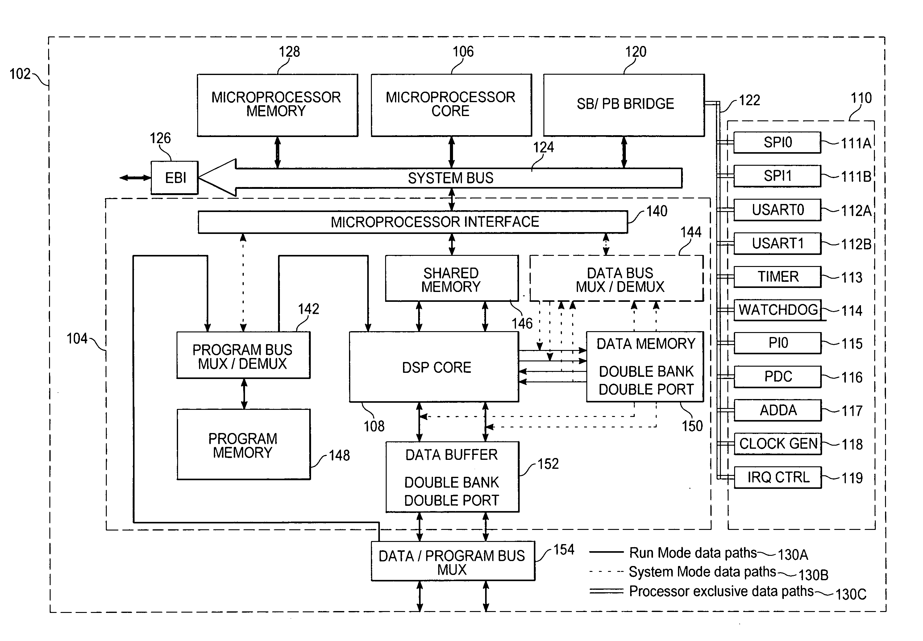
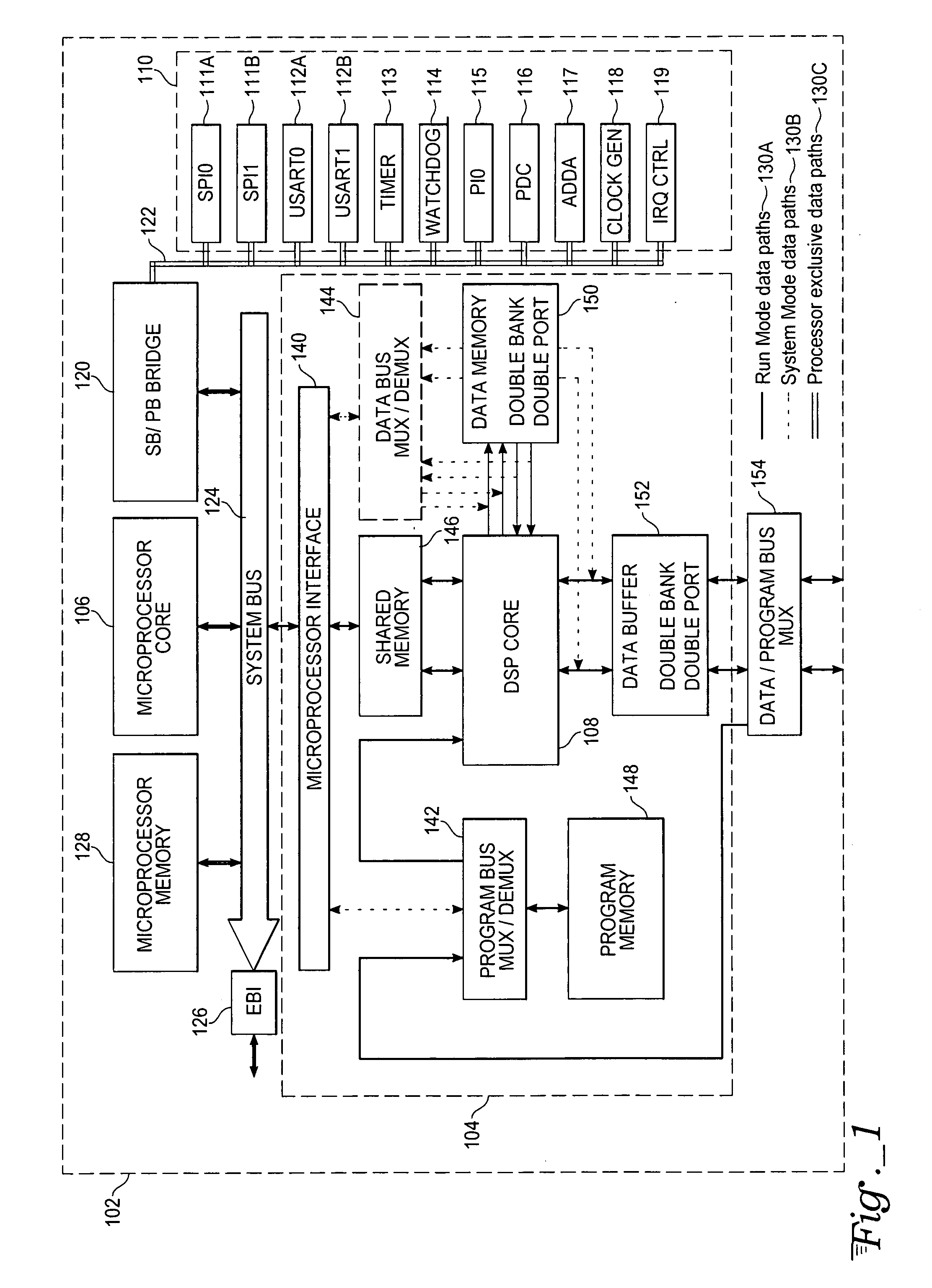
[0032] With reference to FIG. 1, an exemplary embodiment of the general architecture of a system on chip (SoC) 102 includes a floating-point digital signal processor (DSP) subsystem 104, a microprocessor core 106, and a peripheral circuits 110. In a specific embodiment, the microprocessor core 106 is an ARM7TDMI™ ARM Thumb processor core and the floating-point DSP subsystem 104 further comprises a digital signal processor (DSP) core 108 which is an Atmel® mAgic high performance very long instruction word (VLIW) DSP core. The peripheral circuits 110 communicate with a system bus / peripheral bus bridge 120 by means of a peripheral bus 122. The system bus / peripheral bus bridge 120 is coupled to a system bus 124. The system bus 124 is coupled to an external bus interface 126 which generates signals that control access to external memory or peripheral devices. A microprocessor memory 128 is coupled to the system bus 124.

[0033] The system on chip 102 of the exemplary embodiment has two mo...


PUM


Abstract

A system for digital signal processing, configured as a system on chip (SoC), combines a microprocessor core and digital signal processor (DSP) core with floating-point data processing capability. The DSP core can perform operations on floating-point data in a complex domain and is capable of producing real and imaginary arithmetic results simultaneously. This capability allows a single-cycle execution of, for example, FFT butterflies, complex domain simultaneous addition and subtraction, complex multiply accumulate (MULACC), and real domain dual multiply-accumulators (MACs). The SoC may be programmed entirely from a microprocessor programming interface, using calls from a DSP library to execute DSP functions. The cores may also be programmed separately. Capability for programming and simulating the entire SoC are provided by a separate programming environment. The SoC may have heterogeneous processing cores in which either processing core may act as master or slave, or both cores may operate simultaneously and independently.

Description

CROSS-REFERENCE TO RELATED APPLICATION [0001] This application claims priority from Italian Patent Application No. MI2004 A000600, filed Mar. 26, 2004. TECHNICAL FIELD [0002] The invention relates to multiprocessor systems and specifically to a system on chip for digital signal processing with complex domain floating-point computation capability. BACKGROUND ART [0003] The application of digital processing systems to problems of control and computation is rapidly expanding. Advances in the integration of systems on chip (SoC) have made possible a wide variety of new industrial and consumer products and capabilities. A prime example is a cellular telephone. These devices typically utilize a digital signal processor (DSP) to encode voice data, which has been acquired by means of an analog to digital converter, into a binary data stream suitable for transmission over a cellular network. The digital signal processor operates on data in a fixed-point representation. The DSP may be a separ...

Claims


Application Information

Patent Timeline
IPC IPC(8): G06F15/00G06F15/78
CPCG06F15/7864G06F15/7857
Inventor PAOLUCCI, PIER S.ALTIERI, BENEDETTOAGLIETTI, FEDERICOBAZZANA, PIERGIOVANNICERRUTO, ANTONIOCOSIMI, MAURIZIOMICHELOTTI, ANDREAPASTORELLI, ELENARICCIARDI, ANDREA
Owner ATMEL CORP
Why Eureka
Try Eureka