Vacuum processing apparatus and vacuum processing method

a vacuum processing and vacuum processing technology, applied in heat measurement, semiconductor/solid-state device testing/measurement, instruments, etc., can solve the problems of increased investment cost, increased defect, and deterioration of processed samples, so as to reduce investment cost, minimize footprint, and enhance throughput

Inactive Publication Date: 2005-10-06
HITACHI HIGH-TECH CORP
View PDF7 Cites 5 Cited by
  • Summary
  • Abstract
  • Description
  • Claims
  • Application Information

AI Technical Summary

Benefits of technology

[0023] By combining the present multi-chamber system with process modules for etching, annealing, lithography and ashing, and with a defect inspection module or a CD measurement module such as defect review unit, SEM unit or optical appearance inspection device, it becomes possible to inspect every sample for defects inline before and after the process, and the defective sample can be removed from the production lot and recovered in a separate recovery cassette to be subjected to regeneration processes such as washing. Further, by evaluating and processing the samples via inline processing (either in series or in parallel) in a single multi-chamber, the time required for carrying the samples from one apparatus to another and the investment costs for evaluation equipments which were required in the prior art system become unnecessary, and thus, the present invention enables to cuts down investment costs greatly and minimize footprint.
[0024] In other words, according to the present invention, since the inspecting and processing of samples are carried out either in series or in parallel within the same multi-chamber, throughput is enhanced since the conventional time required for carrying the samples among apparatuses is cut down and the individual management of the defective samples is made possible. Further, the defective samples found during inspection are recovered for prompt regeneration, and the investments for separate processing and evaluation facilities are no longer necessary, so the costs invested on facilities can be cut down greatly.

Problems solved by technology

By separately installing an inspection system and a processing system, the time required for carrying samples from one apparatus to another is increased, the output of processed samples is deteriorated, and the investment costs are increased.
Moreover, it is difficult to automatically remove the defective sample within a lot, and the defective sample being subjected to further processing causes the defect to be magnified, and the processed sample will not function as product.
Furthermore, the conventional system cannot carry out in-line inspection for detecting the contamination and process defects caused during and after the processing of samples in the process chamber, and for checking the finished status of the critical dimension of wiring widths and groove widths after the processing.

Method used


Image

  • Vacuum processing apparatus and vacuum processing method
  • Vacuum processing apparatus and vacuum processing method
  • Vacuum processing apparatus and vacuum processing method

Examples


Embodiment Construction

[0028] The preferred embodiments of the vacuum processing apparatus and the vacuum processing method according to the present invention will now be described with reference to the drawings.

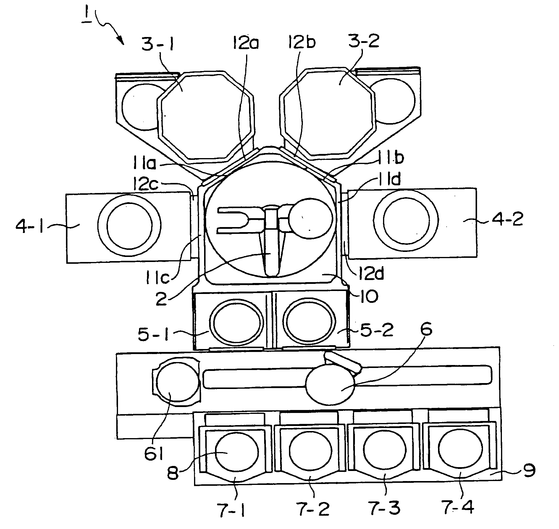
[0029]FIG. 1 is a plan view of a single wafer multi-chamber system for processing wafers in a semiconductor manufacturing facility. A vacuum processing apparatus 1 with single wafer multi-chambers comprises a carrying chamber 10 equipped with a vacuum robot 2 for handling a sample (wafer) 8 to be processed under high vacuum and having two or more coupling ports 11a through 11d disposed to the surrounding walls thereof, process modules 3-1, 3-2 and inspection modules 4-1, 4-2 coupled to the coupling ports 11a through 11d via gate valves 12a through 12d, a load lock chamber 5-1, an unload lock chamber 5-2, an atmospheric loader 6, and a cassette supporting means 9 capable of supporting wafer cassettes. The load lock chamber 5-1 and the unload lock chamber 5-2 can be designed as small capacity chamb...


PUM


Abstract

The invention provides a semiconductor fabrication apparatus capable of preventing increase of carriage time of samples, deterioration of sample output, increase of footprint and increase of investment costs. The vacuum processing apparatus comprises a plurality of vacuum processing chambers 3, 4 for subjecting a sample 8 to vacuum processing; a vacuum carriage means 2 for carrying the sample into and out of the vacuum processing chamber; a switchable chamber 5 capable of being switched between atmosphere and vacuum for carrying the sample into and out of the vacuum processing chamber; a cassette supporting means 9 for supporting a plurality of cassettes 7 capable of housing samples; a carriage means 6 capable of moving vertically for taking out a sample from a given cassette on the cassette supporting means; and a control means performing carriage control for carrying the sample taken out of the given cassette via the carriage means, the switchable chamber and the vacuum carriage means into the vacuum processing chamber, and for carrying the processed sample out of the vacuum processing chamber; wherein the vacuum processing chamber is equipped with an etching chamber 3 and a defect inspection chamber or CD measurement chamber 4 for inspecting the sample for defects.

Description

[0001] The present application claims priority from Japanese patent application No. 2004-097773 filed on Mar. 30, 2004, the content of which is hereby incorporated by reference into this application. FIELD OF THE INVENTION [0002] The present invention relates to a multi-chamber system to be applied to a facility for manufacturing and inspecting semiconductors, electronic components or the like, the system capable of carrying samples such as wafers in vacuum or inert-gas atmosphere by coupling plural process modules and inspection modules organically, thereby integrating manufacturing and inspecting facilities in order to realize cost reduction, high operation efficiency and small footprint. DESCRIPTION OF THE RELATED ART [0003] Heretofore, a multi-chamber semiconductor manufacturing device has been proposed having two cassette chambers, two cleaning chambers and two CVD chambers disposed so as to surround a carrying chamber equipped with a carrier robot (refer for example to patent ...

Claims


Application Information

Patent Timeline
Patent Type & Authority Applications(United States)
IPC IPC(8): H01J37/20H01L21/66H01L21/00H01L21/02H01L21/677H01L21/68
CPCH01L21/67207H01L21/67167
Inventor KAI, YOSHITAKAKUWABARA, KENICHIUCHINO, TAKEONISHIMORI, YASUHIROOONO, TAKESHISHIMADA, TAKESHI
Owner HITACHI HIGH-TECH CORP
Why Eureka
Try Eureka