High-frequency power amplifier circuit and electronic part for communication

a technology of high-frequency power amplifiers and electronic components, which is applied in the direction of amplifiers, amplifiers with semiconductor devices only, amplifiers, etc., can solve the problems of complex control systems, increased circuit scale, and increased gain for a small input signal level, so as to reduce the gain, simplify the control system, and alleviate the effect of signal leakage to the reception frequency band

Inactive Publication Date: 2005-10-06
MURATA MFG CO LTD
View PDF5 Cites 30 Cited by
  • Summary
  • Abstract
  • Description
  • Claims
  • Application Information

AI Technical Summary

Benefits of technology

[0016] A first part of the present invention, which is intended for a wireless communication system having a first operation mode of amplifying a phase-modulated high frequency signal with a high frequency power amplifier circuit and a second operation mode of amplifying a phase and amplitude-modulated high frequency signal with the high frequency power amplifier circuit, is designed to put in a high frequency signal of a fixed amplitude and frequency to the high frequency power amplifier circuit and control the bias states of the amplifying stages of amplifier circuit in accordance with a control signal which is produced by a control circuit based on a demanded output level and detected output level, thereby performing the signal amplification to meet the demanded output level. In consequence, the output level can be controlled by the same control system for both the first and second operation modes without the need of a variable-gain amplifier for the preceding stage of the high frequency power amplifier circuit, whereby the control system can be simplified.
[0017] A second part of the present invention, which is intended for a wireless communication system which requires a linear operation of a high frequency power amplifier circuit, is designed to configure the first-stage amplifier of amplifier circuit with a dual-gate FET or two FETs in serial connection, with an input high frequency signal and a first bias voltage being put in to the first gate terminal of the FET and with a second bias voltage which is higher than the first bias voltage being put in to the second gate terminal, and to create by the first bias voltage such a bias state as to render the linear characteristics to the first-stage amplifier and suppress the gain of the first-stage amplifier by the second bias voltage. In consequence, the high frequency power amplifier circuit has its gain lowered during the linear operation, whereby the signal leakage to the reception frequency band can be alleviated.
[0018] A third part of the present invention, which is intended for a wireless communication system having its output level controlled based on the demanded output level and the output level detected by an output detection means, is designed to include an output level detection means made up of a transistor which receives the input voltage of the last-stage amplifier of the high frequency power amplifier circuit, a current mirror circuit which replicates the transistor current, and a resistor which converts the replicated current into a voltage. In consequence, the amplified output level to be fed back can be detected based on the current detection scheme and a sufficient detection sensitivity is ensured even at a small output level, whereby accurate output control can take place.

Problems solved by technology

However, this manner necessitates a variable-gain amplifier and its control circuit for varying the input signal amplitude in the EDGE mode, resulting in an increased circuit scale (refer to FIG. 2).
Moreover, for the enhancement of modulation accuracy and power efficiency at a small output level, it is necessary to control the bias voltages of the variable-gain amplifier and the high frequency power amplifier circuit simultaneously, resulting in an intricate control system.
However, the gain is too high for a small input signal level, and a resulting amplified noise component gives rise to an increased noise leakage to the reception frequency band which is separated by 20 MHz or more from the transmission frequency.
The study revealed a problem of this scheme when applied to the control of output power by varying the input signal amplitude, with the gate bias voltage being fixed.
Namely, the high frequency power amplifier circuit produces a too small output current variation relative to the DC bias component, particularly at a small output level, and a resulting poor sensitivity of output level detection disables accurate output control and invites the fluctuation of detection level in response to the temperature variation and power voltage variation.

Method used


Image

  • High-frequency power amplifier circuit and electronic part for communication
  • High-frequency power amplifier circuit and electronic part for communication
  • High-frequency power amplifier circuit and electronic part for communication

Examples


Embodiment Construction

[0032] Embodiments of this invention will be explained in detail with reference to the drawings.

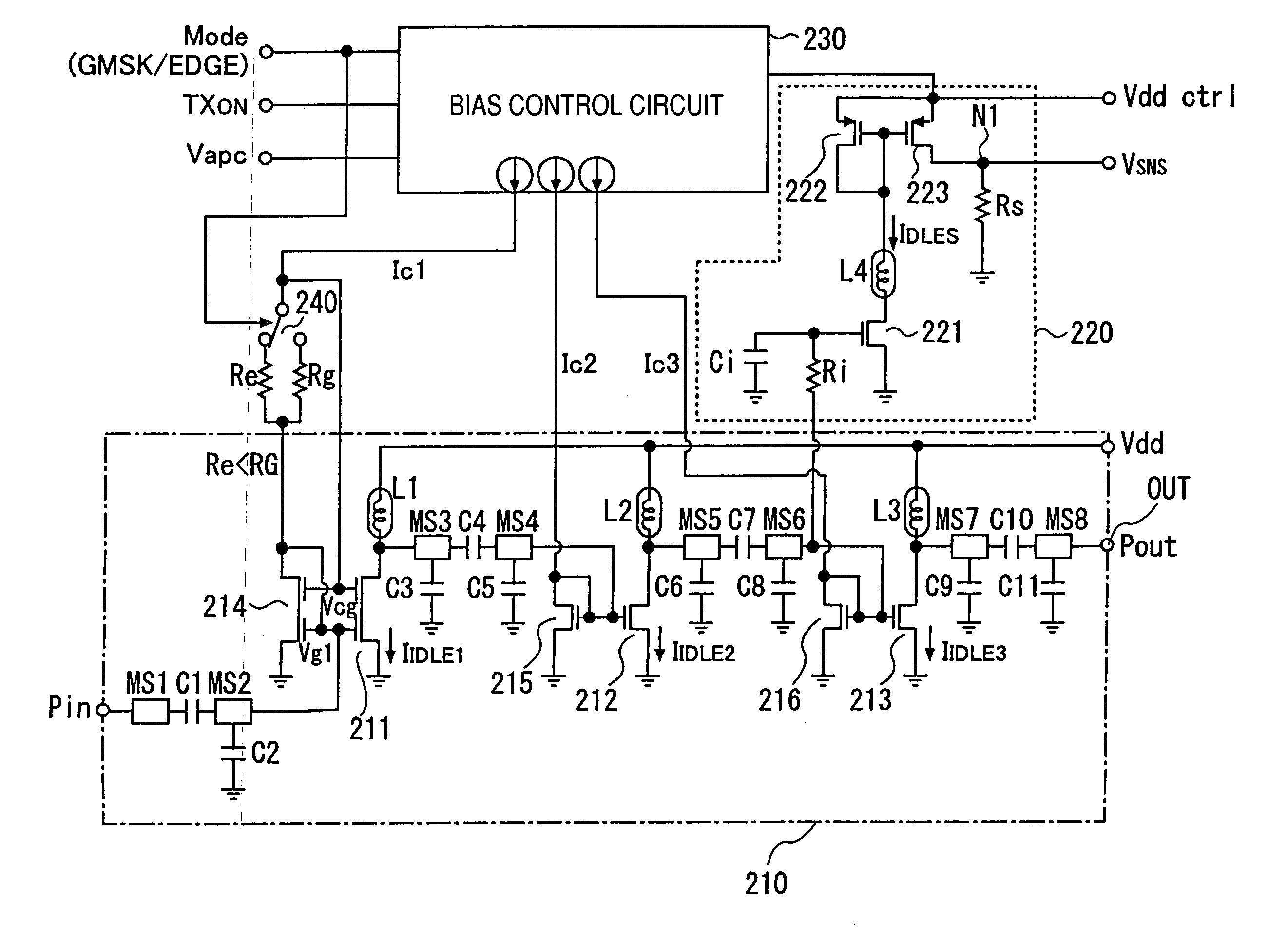
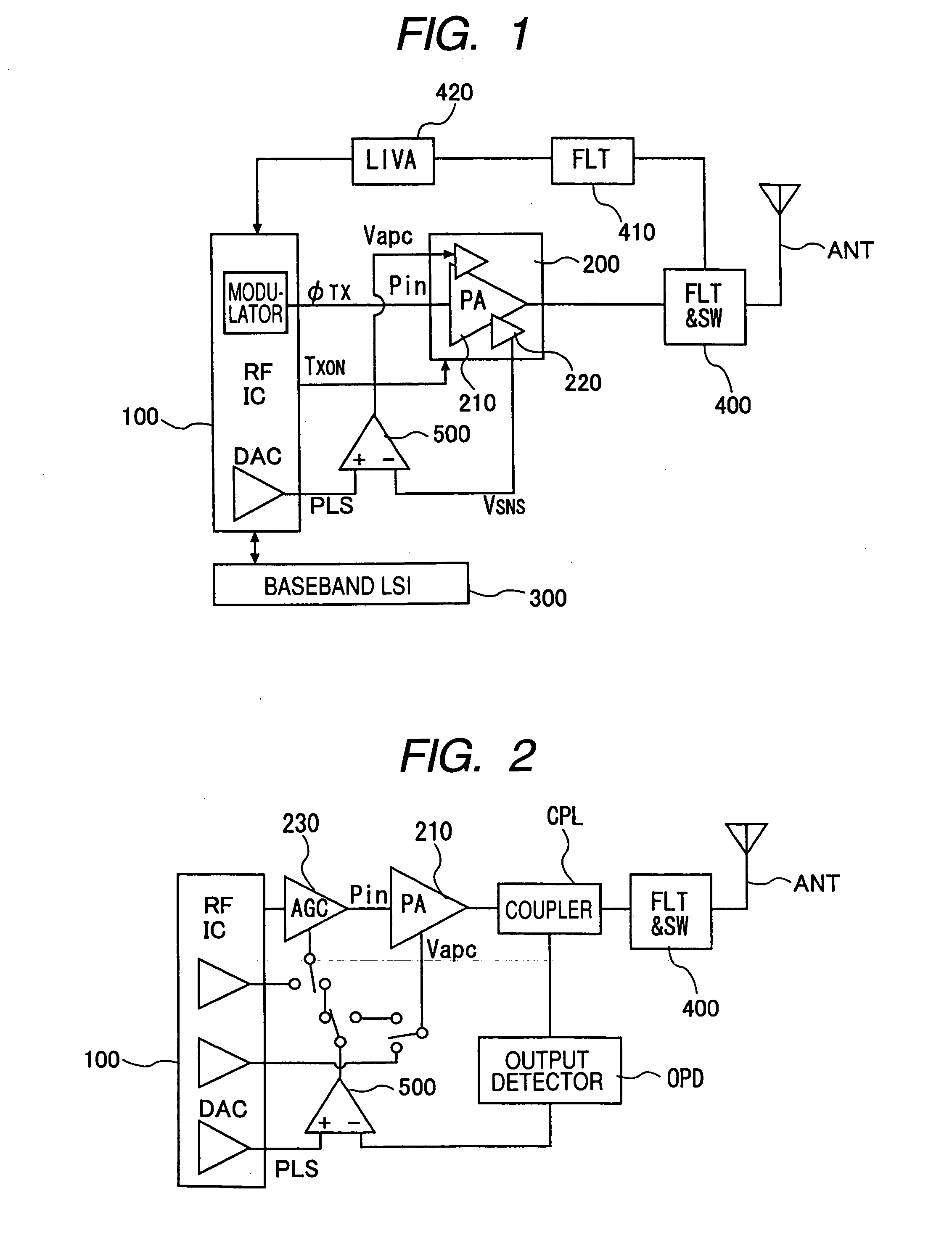
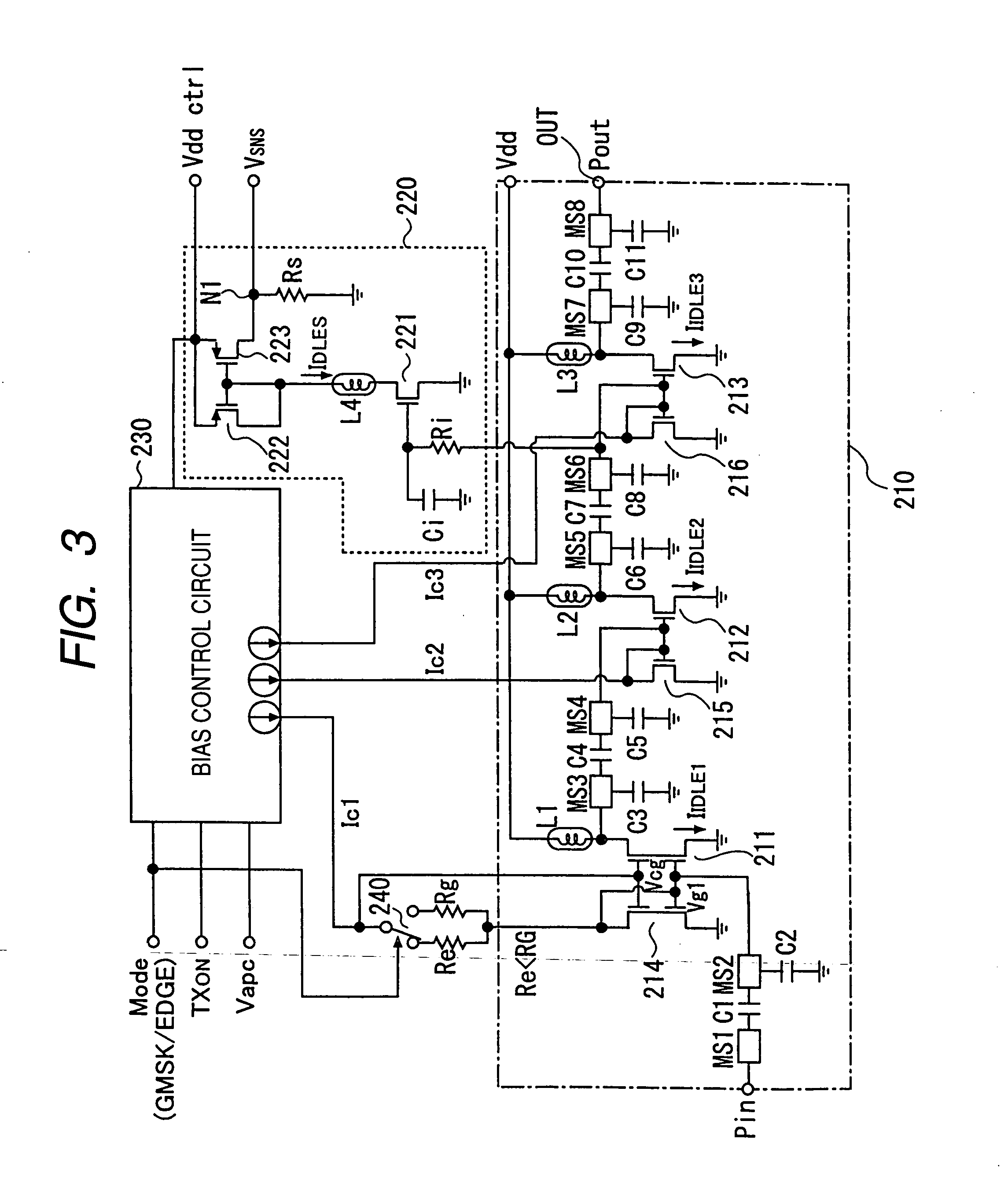
[0033]FIG. 1 shows the arrangement of the transmission system of the wireless communication equipment based on this invention which can perform the EDGE-based communication. The system includes a high frequency IC 100 having a modulation circuit which is designed for GMSK modulation of the GSM scheme and 8-PSK modulation of the EDGE scheme, a power module 200 including a high frequency power amplifier circuit (will be termed simply “power amplifier” hereinafter) 210 used for transmission in unison with an antenna ANT and an output detecting circuit 220 for measuring the transmission power, a baseband circuit in the form of a semiconductor integrated circuit (will be termed “baseband LSI”) 300 for producing an I / Q signal in accordance with sending data (baseband signal) and a control signal for the high frequency IC 100, a front-end module 400 including an impedance matching circuit which...


PUM


Abstract

A wireless communication system has a first operation mode (GSM mode) for amplifying a phase-modulated high frequency signal with a high frequency power amplifier circuit and a second operation mode (EDGE mode) for amplifying a phase and amplitude-modulated high frequency signal with the amplifier circuit. The amplifier circuit has an input of a high frequency signal, with the amplitude and frequency being fixed in both the first and second operation modes, and operates by being controlled for the bias state of each amplifying stage in accordance with the output control signal produced by a control circuit based on the demanded output level (Vapc) and the detected output level (VSNS) so that the amplifier circuit performs signal amplification to meet the demanded output level.

Description

TECHNICAL FIELD [0001] The present invention relates to a high frequency power amplifier circuit for amplifying an input high frequency signal with power amplifying elements which are field effect transistors, and to a technique which can be applied effectively to the wireless communication equipment such as a portable telephone unit which incorporates this high frequency power amplifier circuit. The invention particularly relates to a technique for operating a high frequency power amplifier circuit of the wireless communication equipment at optimal bias conditions in both the operation mode of using the saturation region and the linear operation mode of using the non-saturation region of power amplifying FETs (field effect transistors), and for detecting the output level for feedback control accurately based on the current detection scheme. BACKGROUND ART [0002] Among the conventional schemes of wireless communication equipment (mobile communication equipment) such as portable tele...

Claims


Application Information

Patent Timeline
Patent Type & Authority Applications(United States)
IPC IPC(8): H03F1/02H03F1/06H03F3/193H03G3/20H03G3/30H04B1/04H04B1/40
CPCH03F1/0205H03F1/0272H03F3/193H03F2200/372H04B2001/0416H03G3/3042H03G3/3047H04B1/0475H04B1/406H03F2200/393
Inventor TSUTSUI, TAKAYUKITSUCHIYA, MASAHIROADACHI, TETSUAKI
Owner MURATA MFG CO LTD
Why Eureka
Try Eureka