Magnetoresistive device and method for manufacturing same

a magnetic resistance and magnetic field technology, applied in the field of magnetic resistance devices, can solve the problems of heat resistance and the magnetic field necessary to reverse the direction of the spontaneous magnetization of the free ferromagnetic layer, and achieve the effect of improving the heat resistance of the magnetic resistance devi

Active Publication Date: 2005-10-06
NEC CORP
View PDF9 Cites 46 Cited by
  • Summary
  • Abstract
  • Description
  • Claims
  • Application Information

AI Technical Summary

Benefits of technology

[0014] An object of the present invention is to improve heat res

Problems solved by technology

A problem of the magnetic resistance device utilizing the TMR effect is heat resistance.
Another problem of the magnetic resistance device utilizing the TMR effect is that magnetic field necessary

Method used


Image

  • Magnetoresistive device and method for manufacturing same
  • Magnetoresistive device and method for manufacturing same
  • Magnetoresistive device and method for manufacturing same

Examples


first embodiment

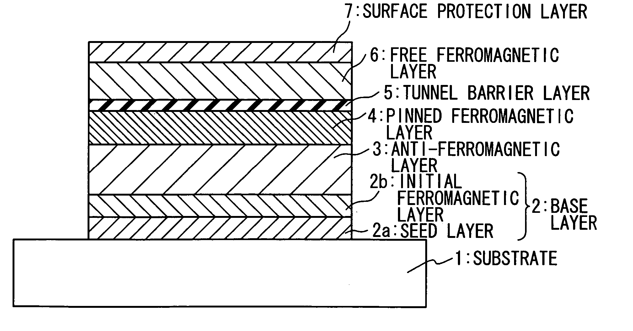
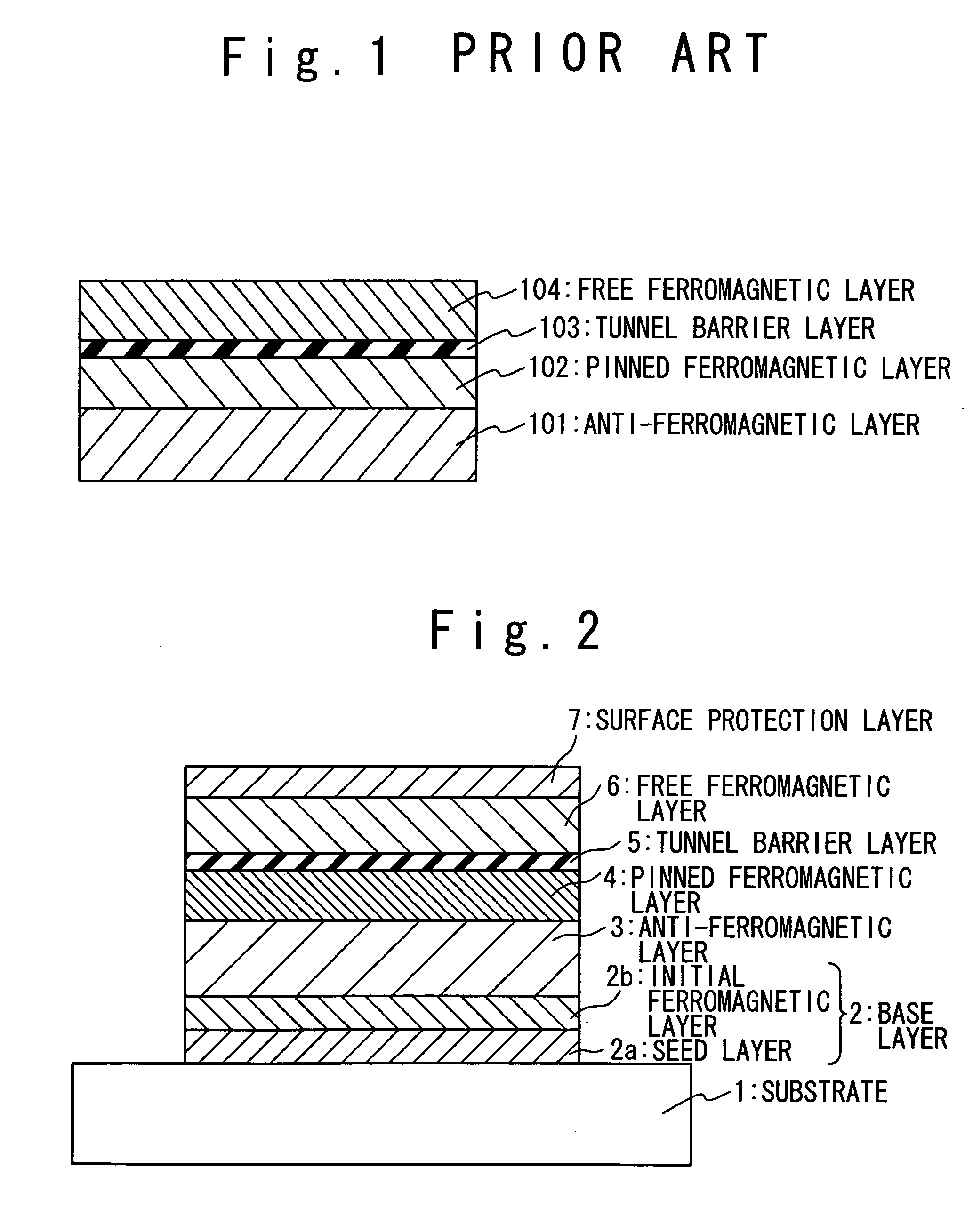
[0041]FIG. 2 shows a magnetic resistance device according to the first embodiment of the present invention. In the magnetic resistance device of the first embodiment, memory cells of a MRAM utilizing the magnetic resistance devices showing TMR effect are provided. The memory cell is composed of a substrate 1 and a base layer 2. The base layer 2 is formed on the substrate 1. The base layer 2 contains a seed layer 2a formed on the substrate 1 and an initial ferromagnetic layer 2b formed on the seed layer 2a. The seed layer 2a is typically formed of tantalum and the initial ferromagnetic layer 2b is formed of Ni—Fe.

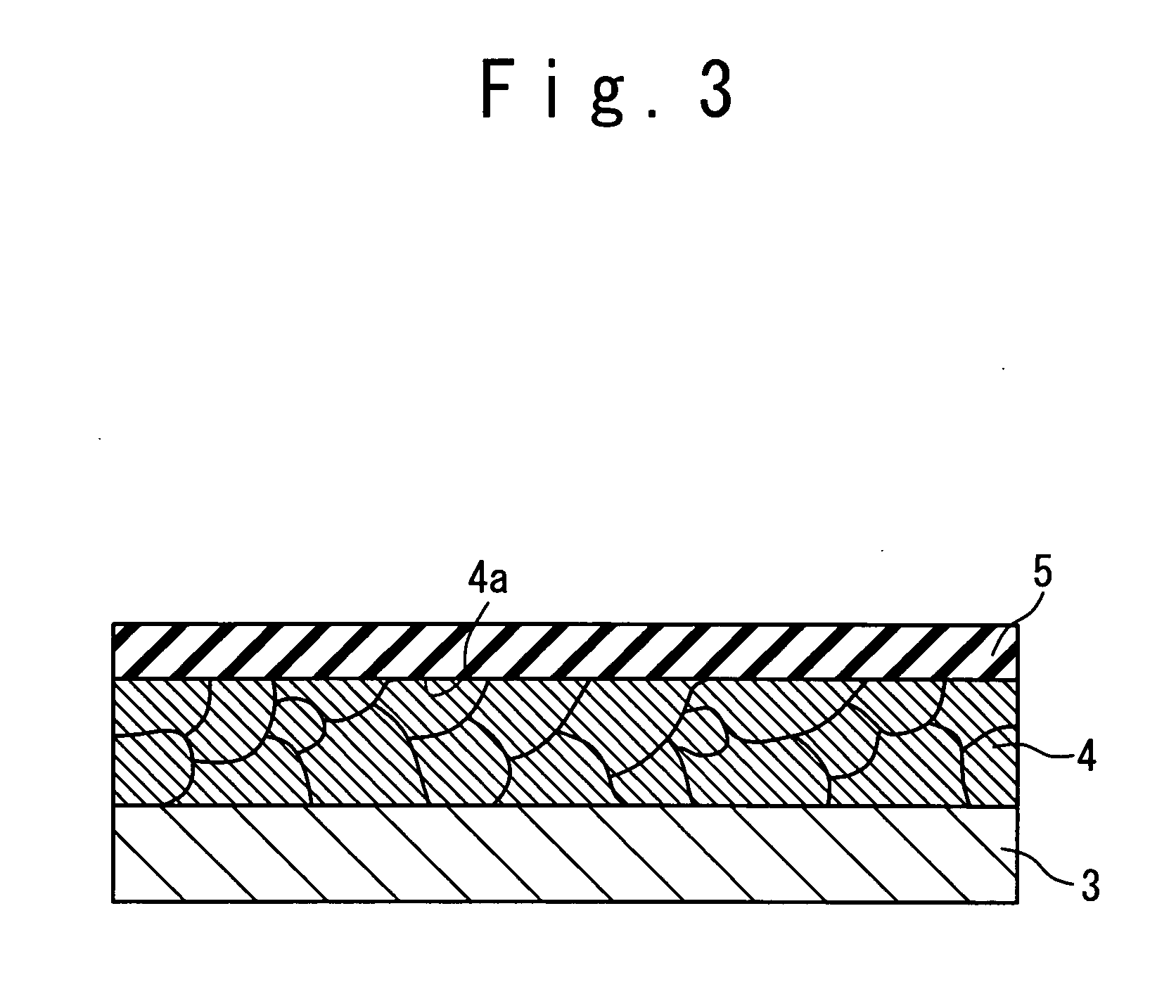
[0042] On the base layer 2, an anti-ferromagnetic layer 3 is formed. For example, the anti-ferromagnetic layer 3 is formed of anti-ferromagnetic material such as Ir—Mn and Pt—Mn. On the anti-ferromagnetic layer 3, a pinned ferromagnetic layer 4 is formed. For example, the pinned ferromagnetic layer 4 is formed of ferromagnetic material such as Ni—Fe and Co—Fe. The pinned fe...

experiment examples

[0053] Experiment examples 1 and 2 as the magnetic resistance device according to the present invention were compared with a comparison example 1. In all of the experiment example 1, the experiment example 2 and the comparison example 1, the seed layer 2a was formed as a tantalum layer having the thickness of 3 nm. The initial ferromagnetic layer 2b was formed as a NiFe layer having the thickness of 3 nm, and the anti-ferromagnetic layer 3 was formed as an IrMn layer having the thickness of 10 nm. Also, the pinned ferromagnetic layer 4 was formed as a CoFe layer having the thickness of 10 nm, and the tunnel barrier layer 5 was formed as an AlOx layer having the thickness of 1.5 nm. The free ferromagnetic layer 6 was formed as a NiFe layer having the thickness of 5 nm, and the surface protection layer 7 was formed as a Ta layer having the thickness of 5 nm.

[0054] The magnetic resistance device of the experiment example 1 was formed by the first manufacturing method of the above-ment...

second embodiment

[0063]FIG. 5 shows a magnetic resistance device according to the second embodiment of the present invention. In the second embodiment, diffusion of the material of the anti-ferromagnetic layer 3 into the tunnel barrier layer 5 is prevented by a different method from that of the first embodiment.

[0064] First, in the magnetic resistance device of the second embodiment, the pinned ferromagnetic layer 11, the non-magnetic layer 12 and the second pinned ferromagnetic layer 13 are formed on the anti-ferromagnetic layer 3 in order. The tunnel barrier layer 5 is formed on the second pinned ferromagnetic layer 13. For example, the first pinned ferromagnetic layer 11 is formed of the ferromagnetic material such as Ni—Fe and Co—Fe. The first pinned ferromagnetic layer 11 formed of the ferromagnetic material has the spontaneous magnetization. The direction of the spontaneous magnetization of the first pinned ferromagnetic layer 11 is fixed through the interaction with the anti-ferromagnetic la...


PUM


Abstract

The heat resistance of a magnetic resistance device utilizing the TMR effect is improved. Also, the Neel effect of the magnetic resistance device utilizing the TMR effect is restrained. The magnetic resistance device includes a first ferromagnetic layer formed of ferromagnetic material, a non-magnetic insulative tunnel barrier layer coupled to the first ferromagnetic layer, a second ferromagnetic layer formed of ferromagnetic material and coupled to the tunnel barrier layer, and an anti-ferromagnetic layer formed of anti-ferromagnetic material. The second ferromagnetic layer is provided between the tunnel barrier layer and the anti-ferromagnetic layer. A perpendicular line from an optional position of the surface of the second ferromagnetic layer passes through at least two of the crystal grains of the second ferromagnetic layer.

Description

TECHNICAL FIELD [0001] The present invention relates to a magnetic resistance device, and more particularly, the present invention relates to a magnetic resistance device with heat resistance improved. BACKGROUND ART [0002] A development is carried forward to apply a magnetic resistance device showing a tunnel magnetic resistance effect (TMR effect) to a magnetic random access memory (MRAM) and a reproduction magnetic head of a high density magnetic recording apparatus. The TMR effect is a kind of magneto-resistance effect. As the magneto-resistance effect, a giant magnetic resistance effect (GMR effect) is known in addition to the TMR effect. However, the TMR effect which shows the magneto-resistance effect larger than the giant magnetic resistance effect (GMR effect) is preferable in application to MRAM and the reproduction magnetic head. [0003] As shown in FIG. 1, the magnetic resistance device showing the TMR effect is typically composed of an anti-ferromagnetic layer 101, a pin...

Claims


Application Information

Patent Timeline
IPC IPC(8): H01F10/12H01F10/30G11B5/39H01F10/32H01F41/18H01F41/20H01L43/08H01L43/12
CPCB82Y10/00B82Y25/00H01L43/12H01F10/3254H01L43/08G11B5/3909H10N50/01H10N50/10
Inventor SHIMURA, KEN-ICHIKAMIJO, ATSUSHIFUKUMOTO, YOSHIYUKIMORI, KAORU
Owner NEC CORP
Why Eureka
Try Eureka