Interconnections for flip-chip using lead-free solders and having reaction barrier layers

a flip-chip and interconnection technology, applied in the direction of electrical equipment, semiconductor devices, semiconductor/solid-state device details, etc., can solve the problems of pb-free applications, the limit of extendibility to larger wafer sizes, and the near-indication of pb-free applications, so as to reduce the occurrence of soft errors in computer chips, the effect of cost-effectiveness

Inactive Publication Date: 2005-10-13
ULTRATECH INT INC
View PDF14 Cites 89 Cited by
  • Summary
  • Abstract
  • Description
  • Claims
  • Application Information

AI Technical Summary

Benefits of technology

[0017] It is another object of the invention to provide flip chip electrical connections that reduce the occurrence of soft errors in computer chips.
[0018] The present invention focuses on cost-effective, environmentally sound, reliable BLM for le

Problems solved by technology

However, it is believed that the limit of extendibility to larger wafer sizes, more de

Method used


Image

  • Interconnections for flip-chip using lead-free solders and having reaction barrier layers
  • Interconnections for flip-chip using lead-free solders and having reaction barrier layers
  • Interconnections for flip-chip using lead-free solders and having reaction barrier layers

Examples


example 1

A Three Layer UBM

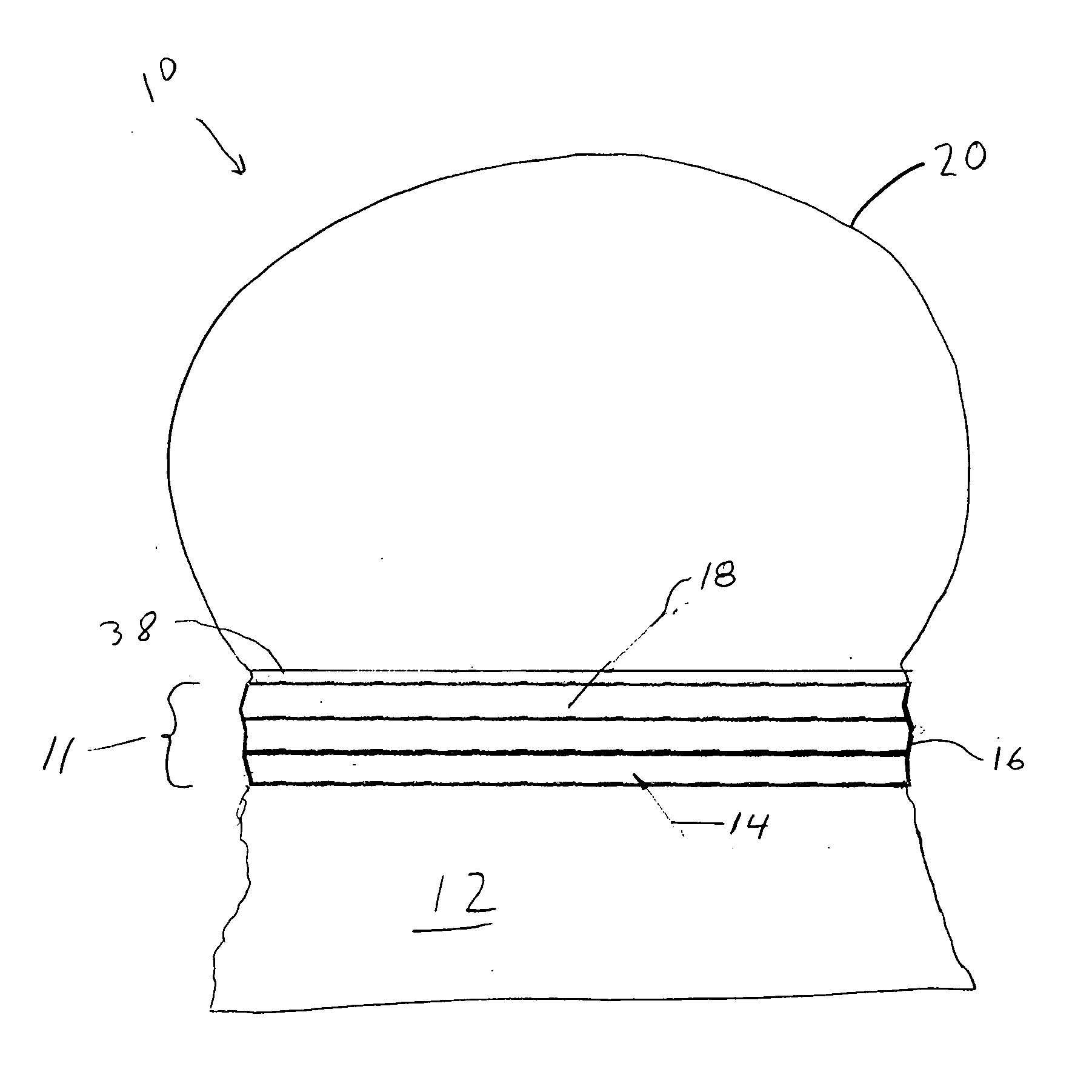
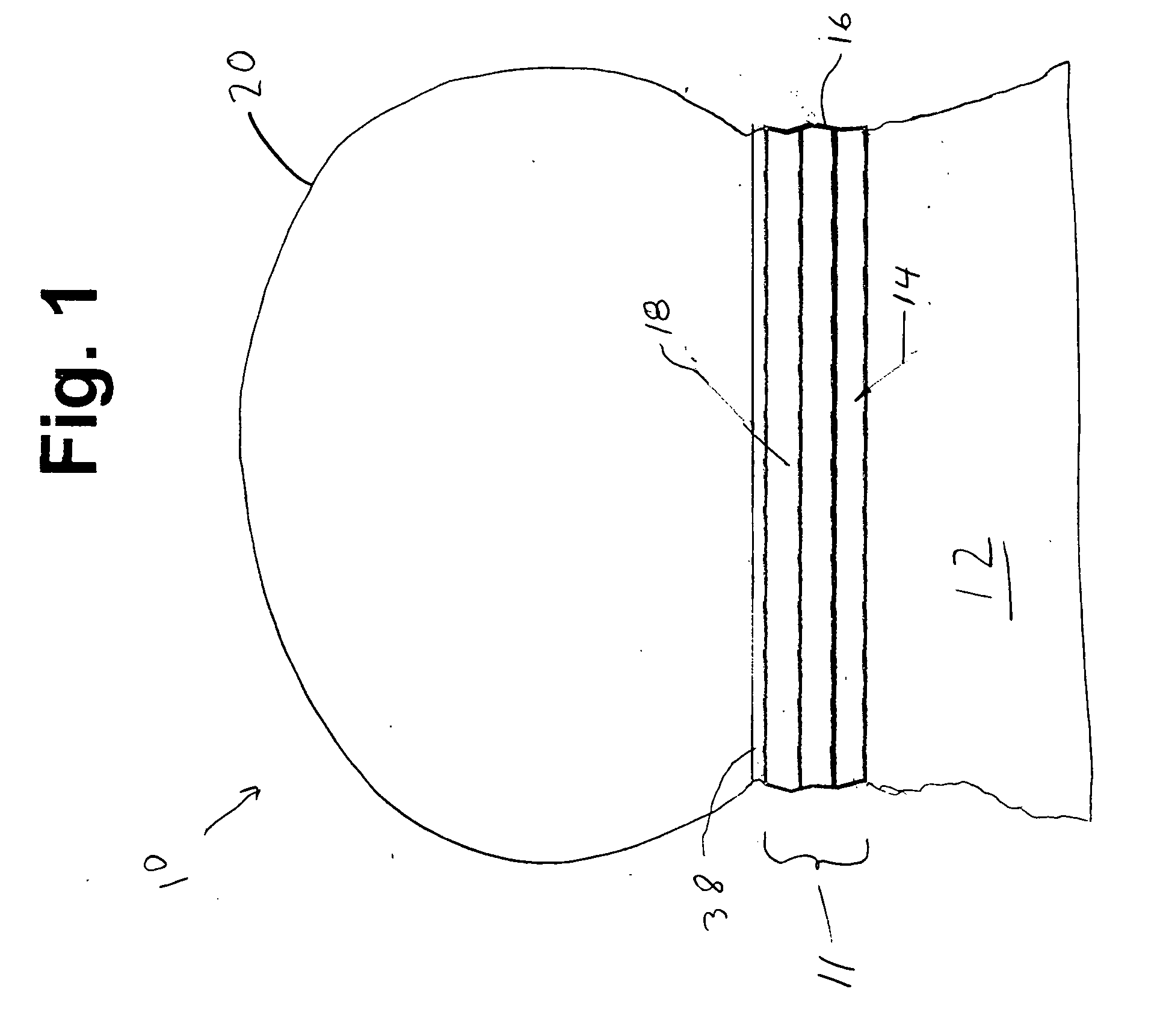
[0040] In accordance with the present invention, a preferred adhesion layer 14 is Cr, TiW or Ti, which is preferably either sputtered or evaporated, at a preferred thickness of about 100 to 3000 angstroms. The thickness of the adhesion layer 12 can vary widely as long as both good adhesion and good barrier properties are maintained. If blanket TiW is deposited and subsequently etched as the final step in forming the patterned BLM structure 11, the film thickness should be minimized consistent with adequate performance. An alternative adhesion layer is Cr or Ti at a thickness of about 100 to 3000 angstroms.

[0041] The second layer 16 is a solder reaction barrier layer, typically a few thousand angstroms to 2 microns in thickness, deposited by sputtering, evaporation or plating. Since the high tin content Pb-free solders are much more reactive than the Pb-rich PbSn solder alloys, Cu, widely used in the high Pb solder, is shown to form thick tin-copper intermetallics ...

example 2

A Four Layer UBM

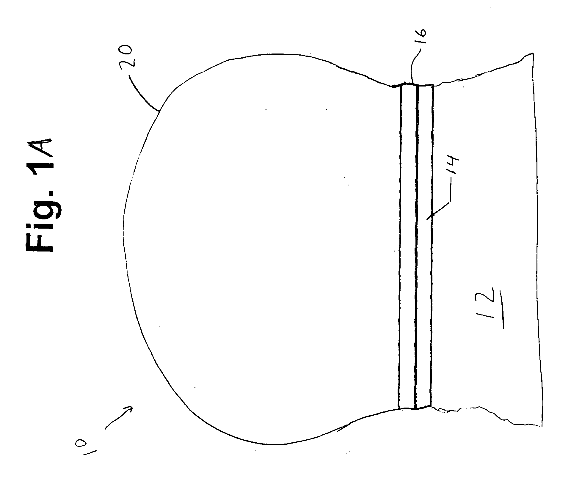
[0047] In this example, the first layer is preferably Cr or TiW. The second layer is preferably Ti, Zr, V, or their alloys (or compounds). The third layer is preferably Cu, CO, Ni, Pd, Pt or their alloys. A fourth layer may be Au or Sn.

example 3

A Simple Two Layer UBM

[0048] In this example, the first layer is preferably Ti which serves both as an adhesion layer and a reaction barrier layer. The second layer is selected from the group consisting of Cu, CO, Ni, Pd, Pt, Sn or their alloys.

[0049] In all three structures Cu is the preferred layer for the reaction, dissolution and incorporation into the solder alloy during reflow joining to form the Sn—Cu or Sn—Ag—Cu solder alloys by simply requiring the plating of the pure Sn or Sn—Ag, respectively, as the bump material.

[0050] The melting properties of the solder alloy that is used over the UBM must be consistent with the requirements of the C4 application. This constraint limits the preferred alloys to those with compositions near the tin-silver eutectic (which contains 2.0-3.8% silver by weight), tin-copper, tin-bismuth, tin-silver-copper ternary eutectic and tin-antimony alloys. The tin-silver eutectic has a melting point of 221 degrees C. and is suitable for this applicat...


PUM


Abstract

An interconnection structure suitable for flip-chip attachment of microelectronic device chips to packages, comprising a two, three or four layer ball-limiting composition including an adhesion/reaction barrier layer, and having a solder wettable layer reactive with components of a tin-containing lead free solder, so that the solderable layer can be totally consumed during soldering, but a barrier layer remains after being placed in contact with the lead free solder during soldering. One or more lead-free solder balls is selectively situated on the solder wetting layer, the lead-free solder balls comprising tin as a predominant component and one or more alloying components.

Description

FIELD OF THE INVENTION [0001] This invention relates to the interconnection of microelectronic integrated circuit (IC) chips to packages, and in particular area-array flip-chip interconnect technology often called C4 (controlled collapse chip connection). The invention further pertains to interconnection schemes that are environmentally acceptable due to the use of lead-free solder alloys and environmentally benign fabrication processes. Further, the invention pertains to interconnection schemes that eliminate sources of soft errors in on-chip circuitry through the elimination of alpha-particle sources in the solder in contact with the microelectronics circuit. BACKGROUND OF THE INVENTION [0002] In the packaging of semiconductor chips, a hierarchy of interconnections is necessary. At the level of the interconnection between the chip and the substrate (or chip carrier), three different interconnection technologies are widely employed: tape automated bonding (TAB), wire bonding, and a...

Claims


Application Information

Patent Timeline
IPC IPC(8): H01L23/48H01L21/60H01L23/485H05K3/34
CPCH01L24/03H01L24/05H01L24/11H01L24/12H01L2224/03912H01L2224/0401H01L2224/1147H01L2224/13023H01L2224/13099H01L2224/131H01L2924/01004H01L2924/01005H01L2924/01006H01L2924/01007H01L2924/01013H01L2924/01014H01L2924/01022H01L2924/01027H01L2924/01028H01L2924/01029H01L2924/0103H01L2924/01033H01L2924/0104H01L2924/01046H01L2924/01047H01L2924/0105H01L2924/01051H01L2924/01073H01L2924/01074H01L2924/01078H01L2924/01079H01L2924/01082H01L2924/01322H01L2924/01327H01L2924/014H01L2924/04941H01L2924/04953H01L2924/14H01L2924/30107H01L2924/00014H01L2224/05H01L2924/01023H01L2924/01024H01L2924/01055H01L2924/01076H01L2224/11849H01L2224/119
Inventor FOGEL, KEITH E.GHOSAL, BALARAMKANG, SUNG K.KILPATRICK, STEPHENLAURO, PAUL A.NYE, HENRY A. IIISHIH, DA-YUANZUPANSKI-NIELSEN, DONNA S.
Owner ULTRATECH INT INC
Why Eureka
Try Eureka