Light source apparatus and optical communication module comprising it

a technology of light source apparatus and optical communication module, which is applied in the direction of electromagnetic transmission, optical resonator shape and construction, and semiconductor lasers. it can solve the problems of large size and considerable power consumption of high-speed optical wireless lan (local area network) products, difficult to achieve scaledown in size and low cost equivalent to those of products conforming to irda, and not yet put to practical use a small-sized inexpensive optical communication module. , excellent electric optical characteristics

Active Publication Date: 2005-10-13
SHARP FUKUYAMA LASER CO LTD
View PDF0 Cites 93 Cited by
  • Summary
  • Abstract
  • Description
  • Claims
  • Application Information

AI Technical Summary

Benefits of technology

[0099] According to the optical communication module, by employing the light source device as the transmission means and further employing, for example, an Si photodiode as a light reception means, there can be provided an optical communication module that satisfies the Class 1 eye safety and concurrently is most inexpensive and excellent in electric optical characteristics for wireless optical communications. Moreover, particularly in an optical communication module, the first region of the multiple scattering optical system is formed as a minute region located adjacent to the light source element (semiconductor laser). Therefore, even when the device

Problems solved by technology

However, the high-speed optical wireless LAN (Local Area Network) products generally have a large size and considerably large power consumption.
Moreover, there have been not a few attempts to use a comparatively inexpensive semiconductor laser of a near infrared wavelength region for wireless optical communications by making the semiconductor laser eye safe attaching importance to the high-speed performance in the past.
However, there have been used comparatively large-scale

Method used


Image

  • Light source apparatus and optical communication module comprising it
  • Light source apparatus and optical communication module comprising it
  • Light source apparatus and optical communication module comprising it

Examples


first embodiment

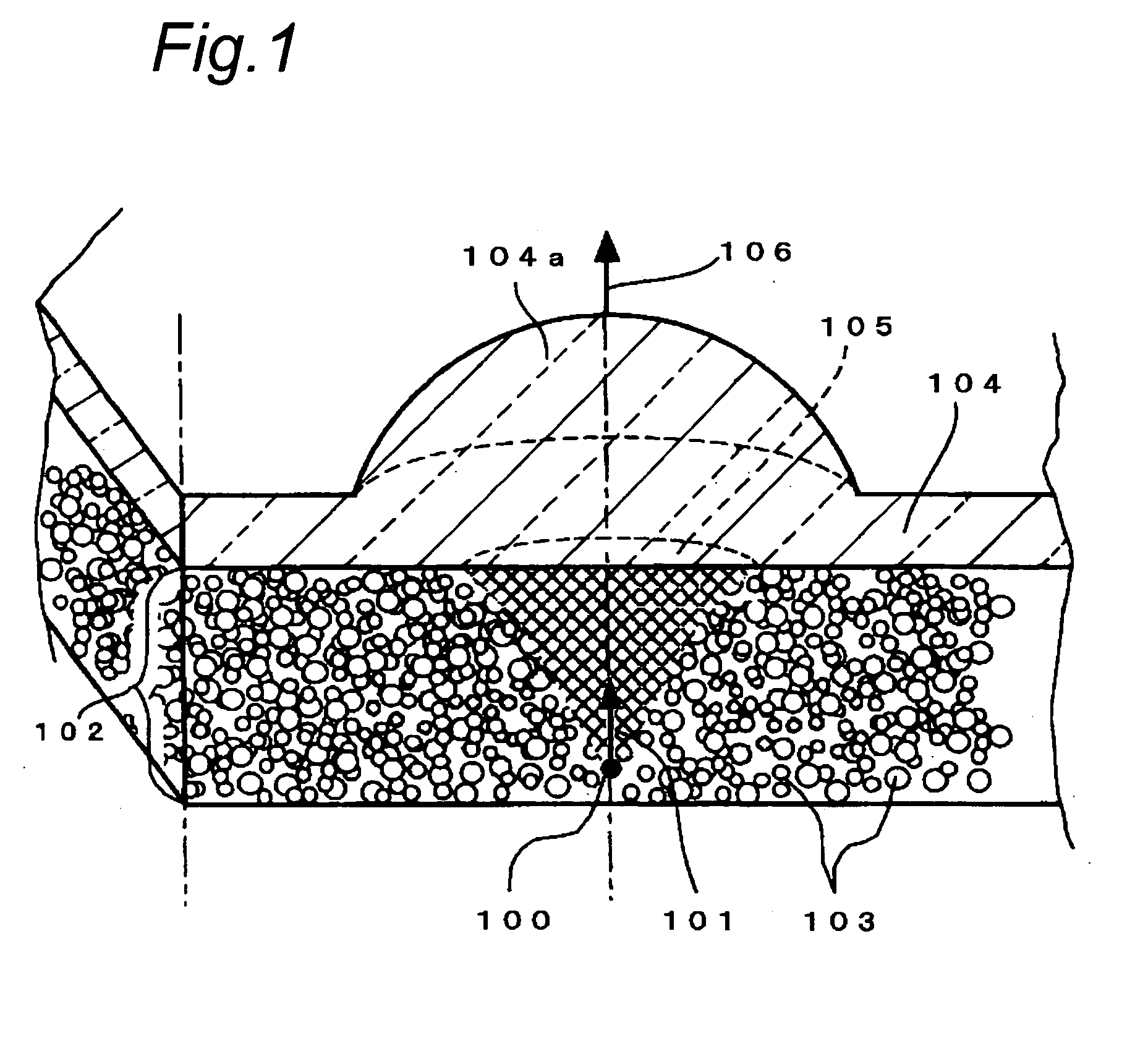
[0131] Dissimilarly from FIG. 1, the first region is also allowed to have a sufficient thickness and intraplanar expansion by directly dripping an appropriate amount of substance that has a comparatively high viscosity in which scatterers are distributed only at the periphery of the semiconductor laser chip.

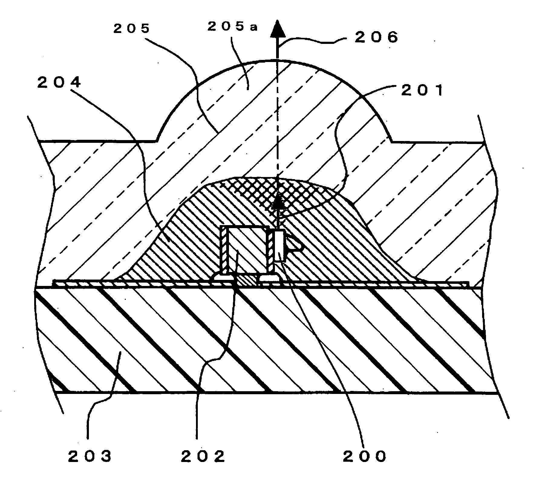
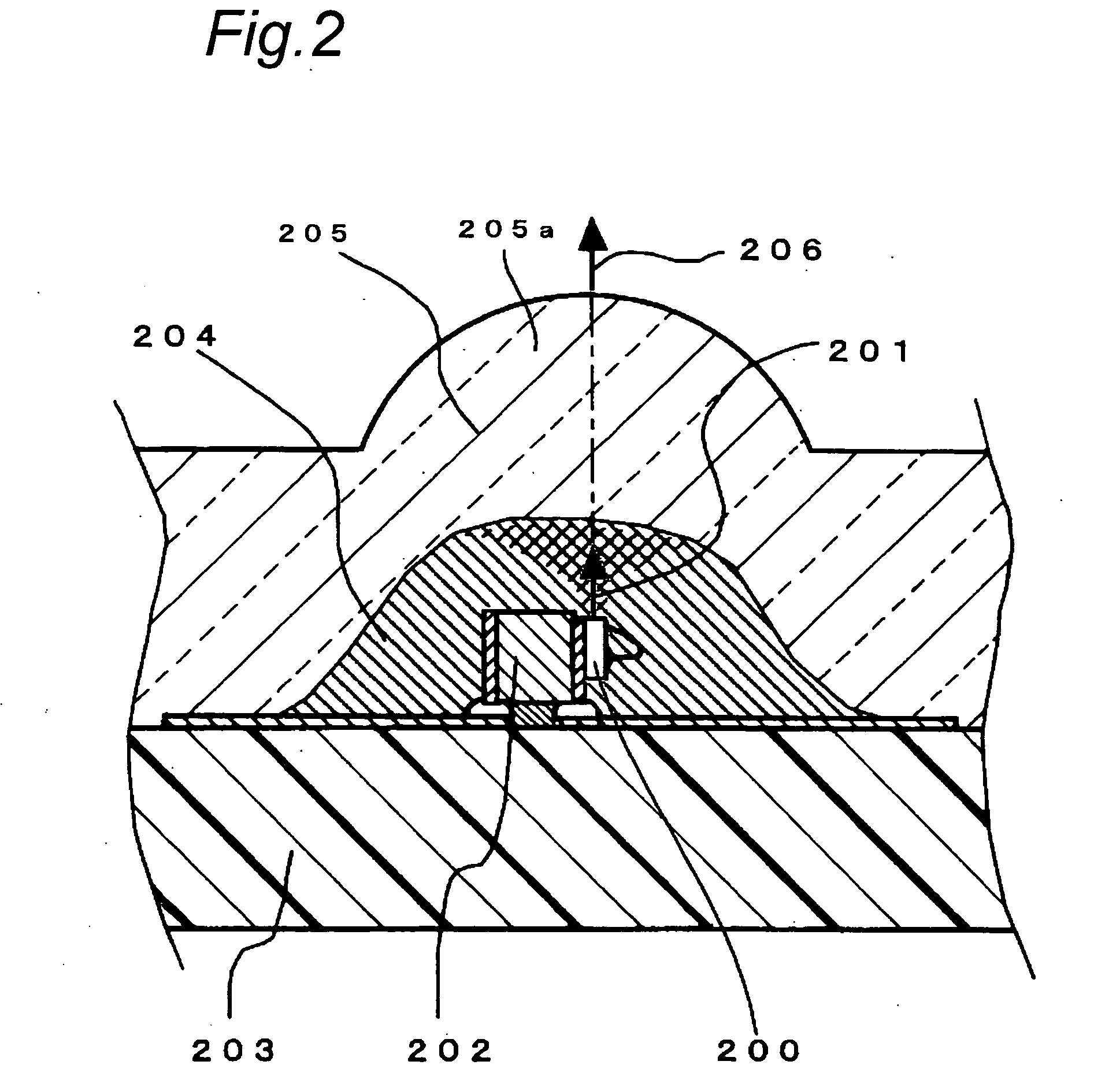
[0132]FIG. 2 is a sectional view showing the construction of an eye-safe light source device that serves as the light source device of the first embodiment of this invention.

[0133] As shown in FIG. 2, a semiconductor laser 200 is die-bonded and wire-bonded to a submount 202 (details are not shown) and mounted on a resin substrate 203 via this submount 202. The optical axis 201 of the semiconductor laser 200 approximately coincides with the optical axis 206 of a lens portion 205a that serves as the magnifier of the second region 205. After the mounting of the semiconductor laser 200 on the submount 202, a paste-like silicone gel having a high viscosity of 30000 cP (30 Pa·s) in w...

second embodiment

[0162]FIG. 4 is a sectional view showing the construction of an eye-safe light source device as the light source device of the second embodiment of this invention. In FIG. 4, the same components as those of the eye-safe light source device shown in FIG. 2 of the first embodiment are denoted by the same reference numerals.

[0163] As shown in FIG. 4, a semiconductor laser 200 is vertically placed on a resin substrate 203 via a submount 202, and thereafter, a cylinder 400 (inside diameter: 1.1 mm, height h=2 mm) is fixed with a silver paste so as to surround the submount 202 on which the semiconductor laser 200 is mounted. As described above, there is formed a recess portion 210 in which the inner surface of the cylinder 400 is served as a wall surface and the surface of the resin substrate 203 is served as a bottom surface. A metal layer 401 is formed by Au plating on the inner peripheral surface of the cylinder 400. An Au plating wiring pattern 402 is formed on the resin substrate 20...

third embodiment

[0173]FIG. 6A is a sectional view showing the construction of an eye-safe light source device that is a third embodiment of the light source device of this invention. FIG. 6B is a schematic view showing the optical path of a semiconductor laser. FIG. 6C is a graph showing the relative light intensity distribution of a near-field pattern.

[0174] A semiconductor laser 600 employed in the eye-safe light source device of this third embodiment was provided by one whose both end surfaces are half-wavelength coated and had a chip thickness of 100 μm, a chip width of 230 μm, a ridge stripe width of 2.5 μm and a cavity length of 500 μm. In this semiconductor laser 600, an InGaAs MQW active layer and AlGaAs-based barrier / guide / cladding layers as used in ordinary 780-nm band lasers are adjusted so that the emission wavelength becomes 890 nm. The semiconductor laser is quite the same as the semiconductor lasers described with reference to FIGS. 2 through 5A, 5B, 5C and 5D of the first and secon...


PUM


Abstract

A light source device for radiating a stimulated emission from a semiconductor laser to outside via a multiple scattering optical system, which system has a first region located adjacent to the semiconductor laser and a second region that abuts on the first region and reaches the outside. The first region contains scatterers at a higher density than the second region does. The light source device has an amount of near-field pattern speckles σPAR of 3×10⁻³ or more. The second region may have a lens portion as a magnifier for at least a principle part of a secondary planar light source formed at an interface between the first and second regions.

Description

TECHNICAL FIELD [0001] The present invention relates to a light source device resin-sealed by transfer molding, potting or the like so that the device is provided with an optical lens function, and to an optical communication module that employs the device. BACKGROUND ART [0002] In recent years, infrared communication modules conforming to the IrDA (Infrared Data Association) standard have been rapidly scaled down in size, and the product of a short distance (20 cm) specification has its lens portion diameter and height reduced to about 1 mm to 2 mm. Concerning the communication speed, there is a gradual increase in speed with regard to IrDA, while compatibilities of a communication distance of several meters with high-speed characteristics of up to about 100 Mbps between a base station where a sufficient quantity of light is provided by arranging parallel twenty or more bullet type LED's and a terminal unit that has a sharp directivity and a tracking function are being established ...

Claims


Application Information

Patent Timeline
IPC IPC(8): H01S5/00H01S5/022
CPCH01S5/005H01S5/02212H01S5/02292H01S5/02288H01S5/02228H01L2224/45144H01L2224/48091H01L2224/48465H01L2224/4848H01L2224/73265H01L2224/8592H01L2924/1815H01S5/02234H01S5/02253H01S5/02255H01L2924/00014H01L2924/00
Inventor HIRAMATSU, TAKUMASHIMONAKA, ATSUSHIMORIMOTO, NAOYUBI
Owner SHARP FUKUYAMA LASER CO LTD
Why Eureka
Try Eureka