Apparatus for biochemical analysis
a biochemical analysis and apparatus technology, applied in the field of integrated devices for biological analyses, can solve the problems of increasing the cost of separate devices, reducing the efficiency of sample processing, and not being useful for dna analysis, and achieve excellent thermal response and high thermal conductivity
- Summary
- Abstract
- Description
- Claims
- Application Information
AI Technical Summary
Benefits of technology
Problems solved by technology
Method used
Image
Examples
example 1
Integrated Device for Biochemical Analysis
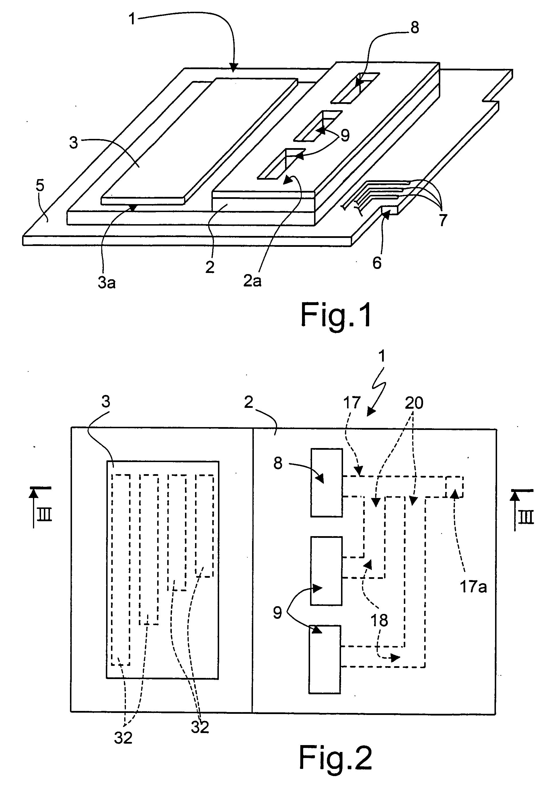
[0043] As illustrated in FIG. 1, an integrated device for DNA analysis (Lab-On-Chip) designated, as a whole, by the reference number 1, comprises a microreactor 2 and a micropump 3. The microreactor 2 is carried on a printed-circuit board (PCB) 5 equipped with an interface 6 for connection to a driving and reading device (not illustrated herein). In particular, input / output pins 7 of the microreactor 2 and of the micropump 3 are provided on the interface 6.
[0044] The microreactor 2 has a specimen tank 8 and a plurality of reagent tanks 9 (two, in the example illustrated), which are open on one face 2a opposite to the PCB base 5 and accessible from outside. The micropump 3 is hermetically seal-welded on the microreactor 2 (see also FIG. 2).
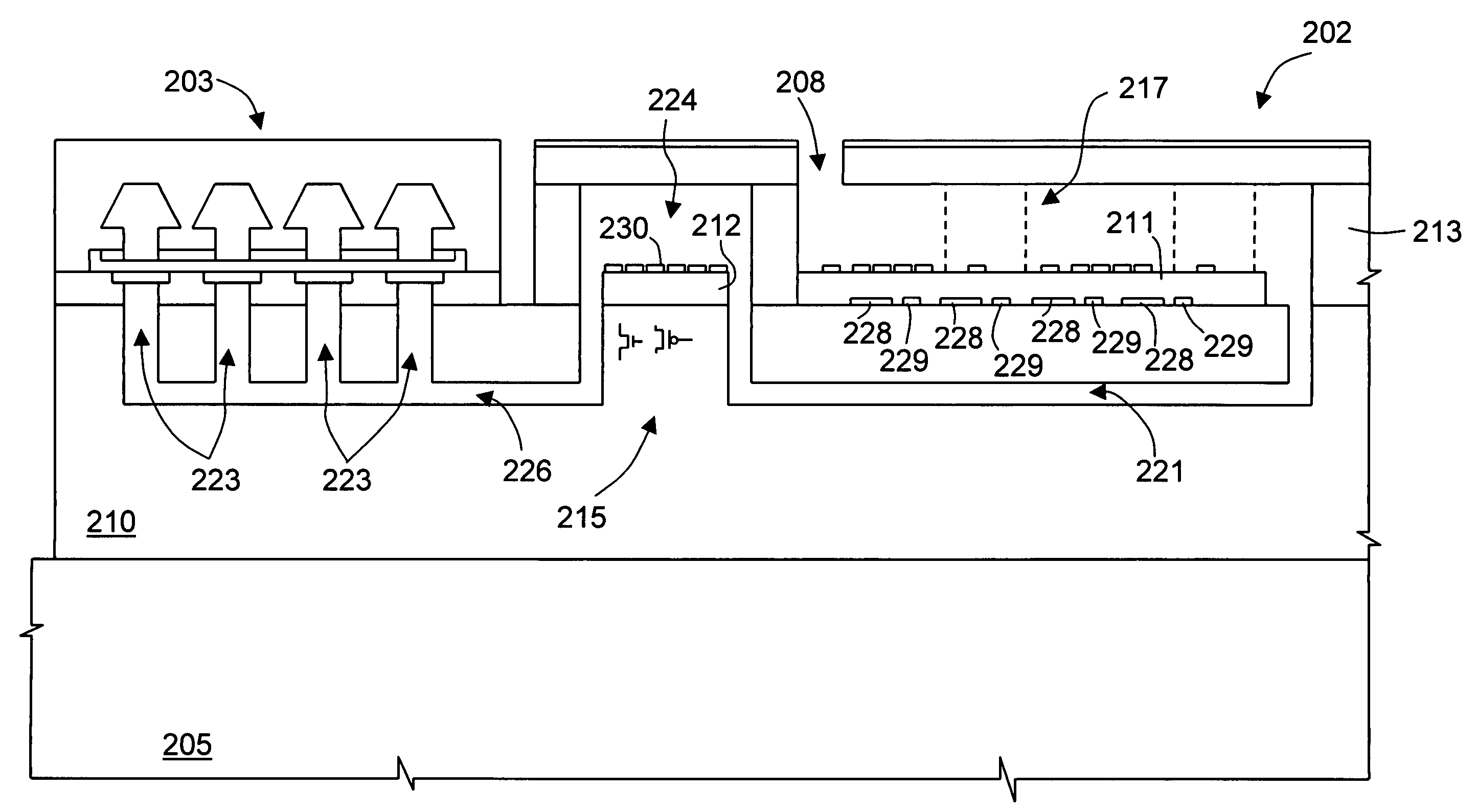
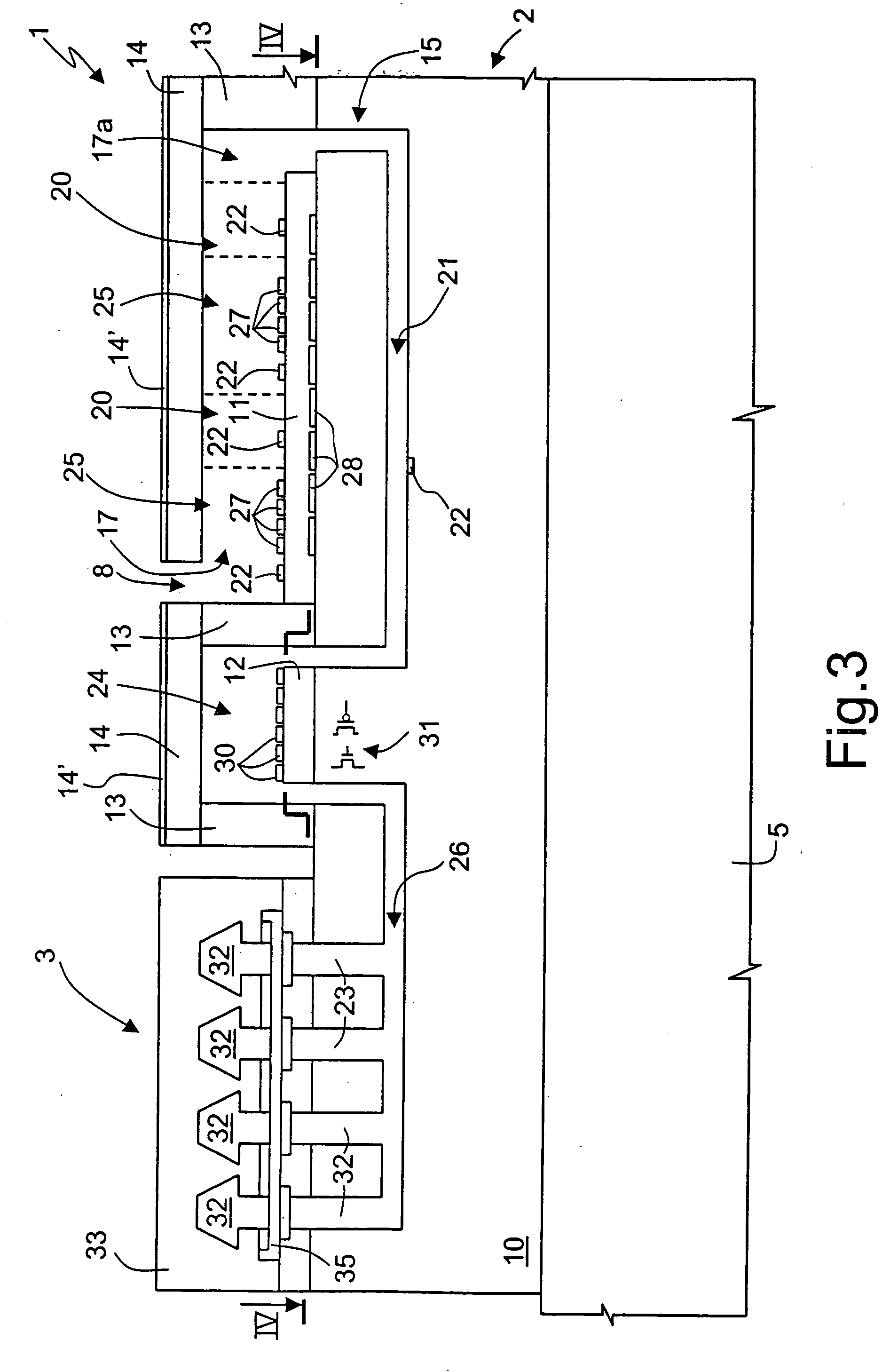
[0045] With reference to FIGS. 3 and 4, the microreactor 2 comprises a first body 10 of semiconductor material, for instance, monocrystalline silicon, and, on top thereof, a first and a second base 11, 1...
example 2
Manufacture of Integrated Device
[0079] Both the microreactor 2 and the micropump 3 can be implemented in a simple way. In particular, a process for manufacturing the microreactor 2 is illustrated hereinafter with reference to FIGS. 10 to 13.
[0080] The amplification channel 21, and the suction channel 26, buried in the substrate 51, and the chimneys 23 are formed. Next (see FIG. 11), after depositing a polysilicon germ layer, not illustrated here, that is removed from the portion of the substrate 51 where electronic components are to be integrated, an epitaxial layer 52 is grown and oxidized on the surface. Then, the CMOS sensor 31 is formed in the monocrystalline portion of the wafer 50; a pad oxide layer 53 is formed, and the heater 28 is deposited thereon. The substrate 51 and the epitaxial layer 52 in practice form the supporting body 10 of the microreactor 2.
[0081] Next (see FIG. 12), a thick layer of silicon dioxide is deposited and defined so as to form the first base 11 an...
example 3
Prototype Temperature Profile
[0101] A prototype silicon channel was made by bonding 2 etched silicon wafers to produce a 600 μm wide lozenge shaped channel. A thermocouple was inserted into the channel under oil and the chip placed on a thermo-cycler. Thermal profiles were compared with a regular plastic PCR tube in the same thermo-cycler as shown in FIG. 22. The results confirm that a silicon substrate provides superior thermal performance due to its high thermal conductivity. This will allow the cycling times to be minimized for fastest performance.
PUM
| Property | Measurement | Unit |
|---|---|---|
| Temperature | aaaaa | aaaaa |
| Semiconductor properties | aaaaa | aaaaa |
Abstract
Description
Claims
Application Information


