Semiconductor laser apparatus and manufacturing method thereof

a semiconductor laser and diode technology, applied in semiconductor lasers, electrical devices, laser details, etc., can solve the problems of inability to conduct normal operation, insufficient esd countermeasures, and increased esd breakdown voltage, so as to improve the resistance to static voltage breakdown and high reliability

Active Publication Date: 2005-10-27
FUJIFILM BUSINESS INNOVATION CORP
View PDF6 Cites 43 Cited by
  • Summary
  • Abstract
  • Description
  • Claims
  • Application Information

AI Technical Summary

Benefits of technology

[0012] The present invention addresses the problems in the prior art to improve the resistance to static voltage breakdown by integrating a vertical-cavity surface-emitting laser diode and a protective device and provide a semiconductor laser apparatus of high reliability and a manufacturing method thereof.

Problems solved by technology

If electrostatic discharge (hereinafter referred to as ESD) should occur inside the device, since a large spike current flows instantaneously, this destroys or deteriorates the device causing a failure not capable of conducting normal operation.
According to the result, it is considered that ESD damage is a function of an oxidized aperture diameter or area and the ESD breakdown voltage increases as the oxidized aperture diameter increases.
However, the existent protective device for the VCSEL has the following problems.
Hei 11-112026, in a case of handling the light emitting device as a single component, the ESD countermeasure is still insufficient.
Further, this increases the number of elements constituting the laser device to increase the cost.
Integration of VCSEL and the protective diode on one chip in U.S. Pat. No. 6,185,240B1 may be a countermeasure for ESD during handling, but plural trenches have to be formed when the protective diode is formed on the substrate, which complicates the steps and cannot always form the diode easily.
While Bobby M. Hawkings, et al., “Reliability of Various Size Oxide Aperture VCSELs” Honeywell, 2000 shows that the ESD withstand voltage increases in proportion with the oxidized aperture diameter, desired basic laser characteristics cannot be obtained by merely increasing the oxidized aperture diameter.
Particularly, in a single mode VCSEL, the oxidized aperture diameter tends to be decreased, which inevitably lowers the ESD withstand voltage.

Method used


Image

  • Semiconductor laser apparatus and manufacturing method thereof
  • Semiconductor laser apparatus and manufacturing method thereof
  • Semiconductor laser apparatus and manufacturing method thereof

Examples


third embodiment

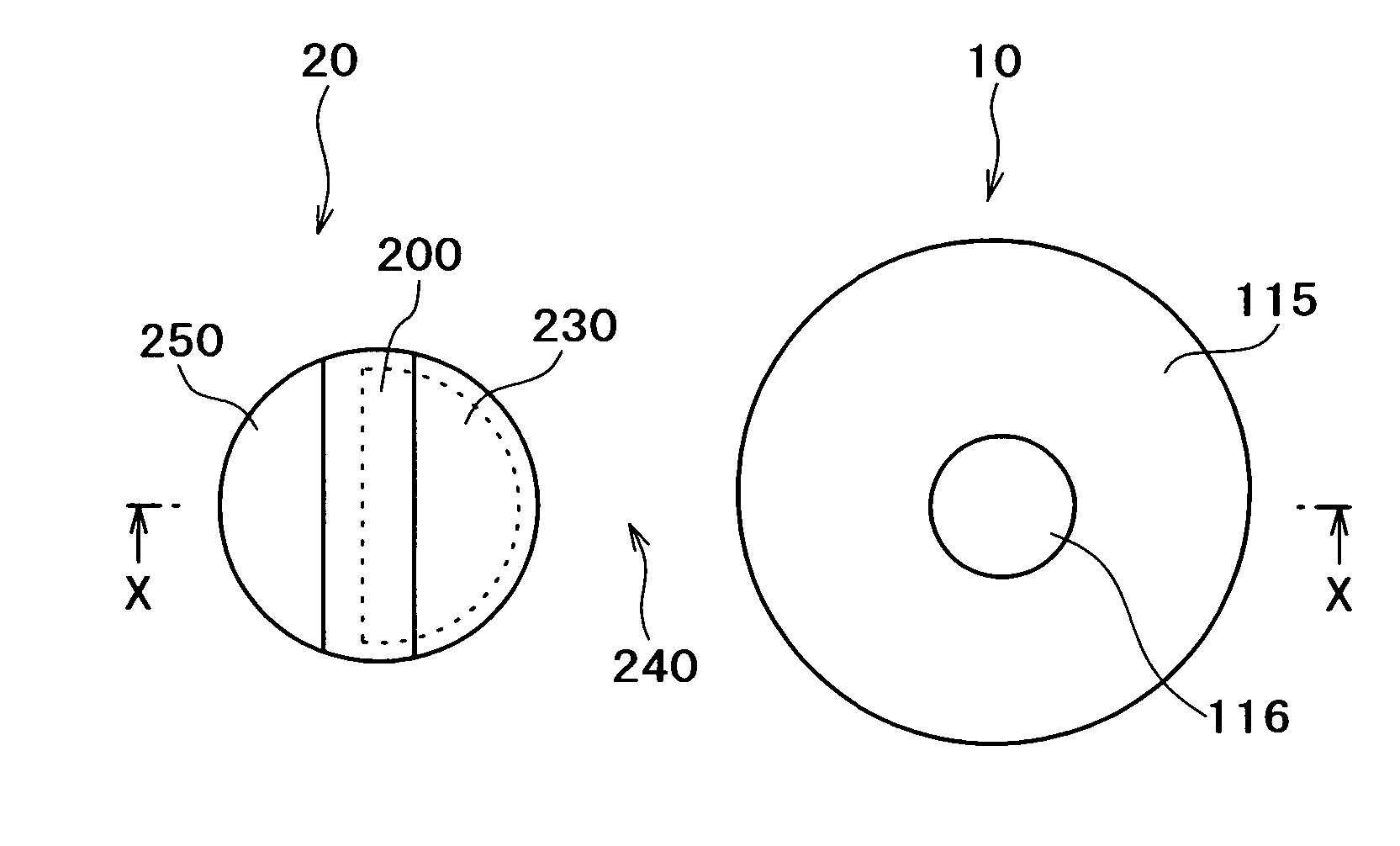
[0039]FIG. 5 shows a modification of the third embodiment in which electrical contact is established with a portion of a lower DBR mirror layer 103 formed on the substrate instead of using the n-side electrode layer 117 at the back of the substrate 101. An electrode layer 250 of a Zener diode 22 is electrically connected by way of the contact hole 310 in an interlayer insulation film 113 to the n-type semiconductor layer of the lower DBR mirror 103. The anode electrode of the Zener diode 22 and the cathode electrode of the VCSEL 10 may be connected in this manner. Further, an n-type contact layer 330 may be present in the lower DBR mirror 103 and the contact layer 330 and the electrode layer 250 may be connected. In this case, a material may be selected for the contact layer 330 such that the reflectivity of the lower DBR mirror layer is not lowered.

first embodiment

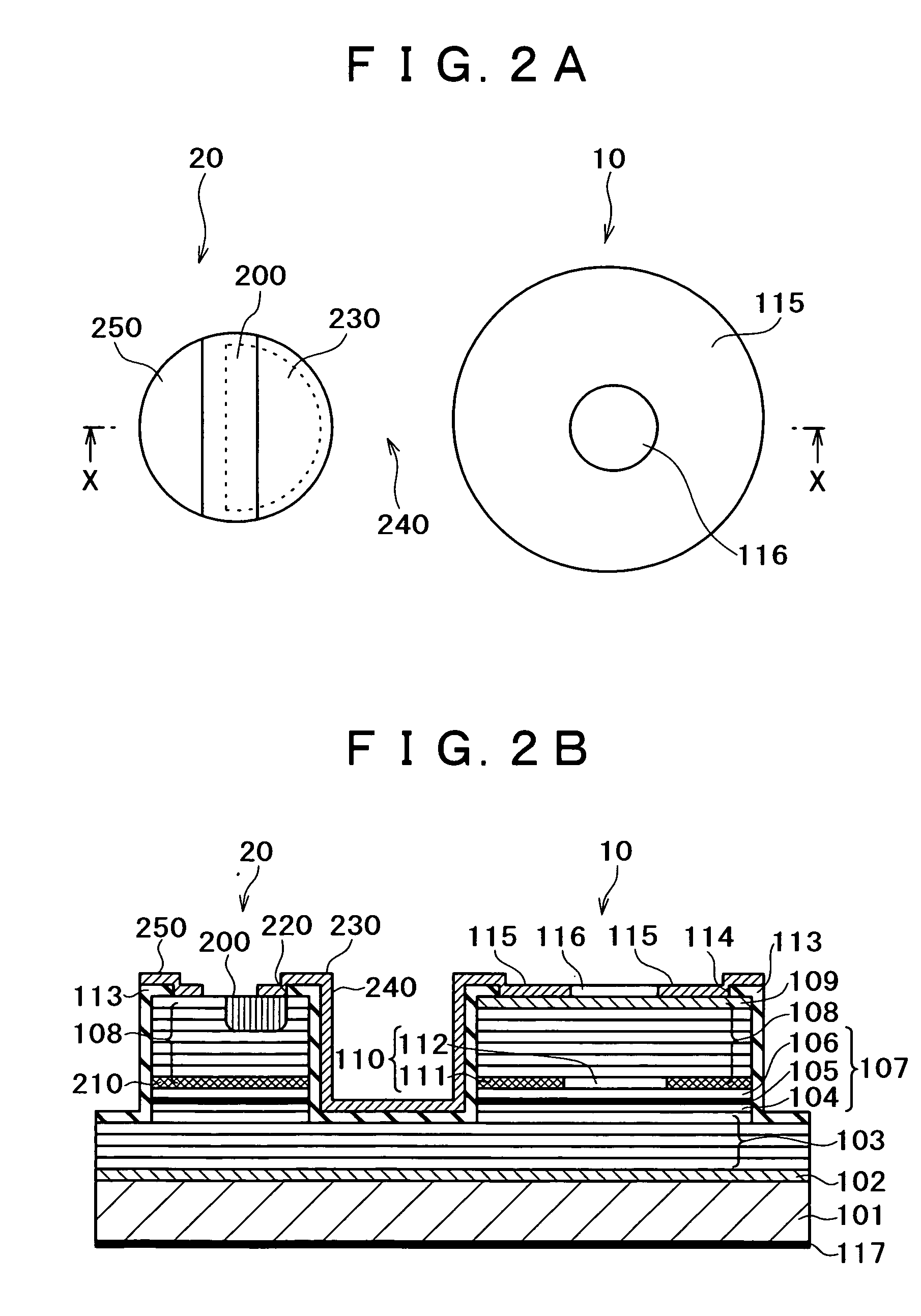
[0040] Then, the steps of manufacturing a semiconductor laser apparatus is to be described with reference to FIGS. 6A to 6C, 7A to 7C, 8A and 8B. As shown in FIG. 6A, plural semiconductor layers are stacked on the substrate 101 by use of a metal organic chemical vapor deposition method (MOCVD). That is, on the n-type GaAs substrate 101, the n-type buffer layer 102, an n-type lower DBR mirror layer 103, active layer 107 containing the undoped lower spacer layer 104, undoped quantum well active layer 102 and undoped upper spacer layer 106, and p-type upper DBR mirror layer 108 containing the contact layer 109 and AlAs layer (current confining layer) 110 are stacked successively.

[0041] The lower DBR mirror layer 103 is a multi-layered stack including an n-type Al0.9Ga0.1As layer and an n-type Al0.3Ga0.7As layer with the thickness of each layer being λ / 4nr (in which λ represents an oscillation wavelength and nr is a refractive index of a medium) and the layers are stacked alternately a...


PUM


Abstract

A semiconductor laser apparatus includes a substrate, a vertical-cavity surface-emitting semiconductor laser diode (VCSEL) including a first and second mirror layers of a first and second conduction types, respectively, an active region between the first and second mirror layers, a first and second electrode layers electrically connected with the first and second mirror layers, respectively, and at least one Zener diode including a first and second semiconductor regions of a first and second conduction types, respectively, and a third and fourth electrode layers electrically connected with the first and second semiconductor regions, respectively. The second semiconductor region is formed in a portion of the first semiconductor region and forms a PN junction with the first semiconductor region. The VCSEL and the Zener diode are formed on the substrate. The first and second electrode layers are electrically connected with the fourth and third electrode layers, respectively.

Description

BACKGROUND OF THE INVENTION [0001] 1. Field of the Invention [0002] The present invention concerns a vertical-cavity surface-emitting laser diode (hereinafter referred to as VCSEL) and, it specifically relates to a protective structure for protecting the VCSEL against electrostatic damage. [0003] 2. Description of the Related Art [0004] The VCSEL has excellent features in that it has low threshold current, small power consumption and can obtain a circular light spot easily, and light sources can be arranged as a two-dimensional array, and it has been expected for use as a light source in optical communication equipment or electronic equipment. [0005] Like other semiconductor devices, the VCSEL is sometimes exposed to a high voltage by static electricity in handling of circuit substrates, etc. If electrostatic discharge (hereinafter referred to as ESD) should occur inside the device, since a large spike current flows instantaneously, this destroys or deteriorates the device causing a...

Claims


Application Information

Patent Timeline
Patent Type & Authority Applications(United States)
IPC IPC(8): H01S5/00H01S5/026H01S5/068H01S5/183H01S5/30
CPCH01S5/0261H01S5/06825H01S5/3054H01S5/305H01S5/18313
Inventor KUWATA, YASUAKINAKAYAMA, HIDEOMURAKAMI, AKEMIISHII, RYOJI
Owner FUJIFILM BUSINESS INNOVATION CORP
Why Eureka
Try Eureka