

Silicon single crystal wafer and epitaxial wafer, and method for producing silicon single crystal
a single crystal and silicon technology, applied in the field of silicon single crystal, can solve the problems of oxide dielectric breakdown voltage characteristic and device characteristics, oxide-film defects remarkably, and deformation of electrical characteristics, so as to improve the yield of devices and excellent electrical characteristics and gettering ability
- Summary
- Abstract
- Description
- Claims
- Application Information
AI Technical Summary
Benefits of technology
Problems solved by technology
Method used
Image

Examples
experiment 1
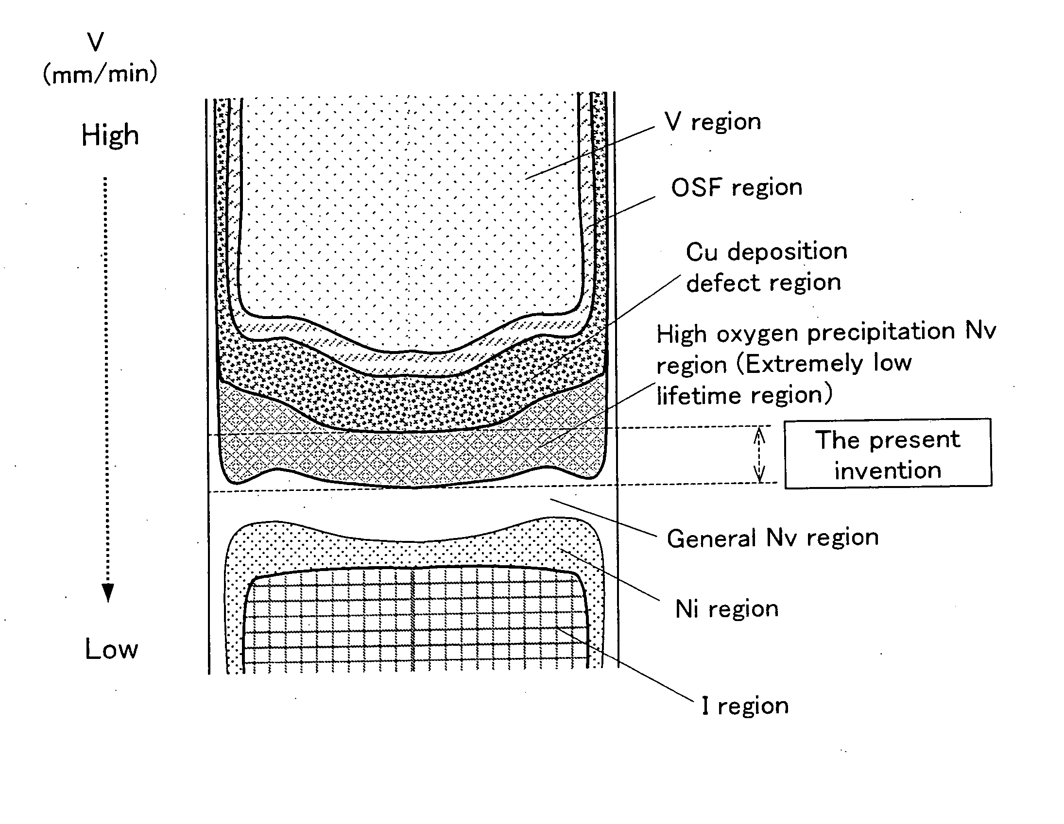
(Experiment 1): Confirmation of High Oxygen Precipitation Nv Region
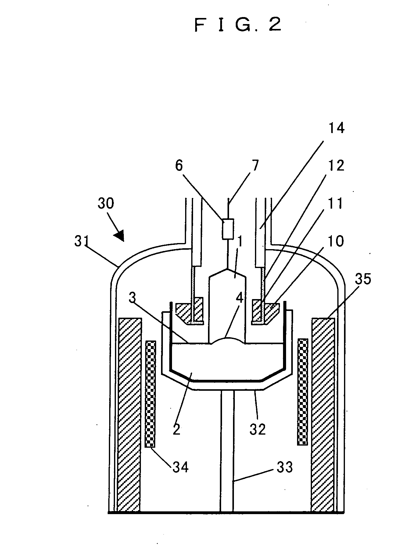
[0076] An experiment on gradual lowering of a crystal growth rate was carried out as explained below using the apparatus 30 for manufacturing a single crystal shown in FIG. 2 to research growth rates at boundaries of respective regions.
[0077] 120 kg of polycrystalline silicon as a raw material was charged into a quartz crucible having a diameter of 24 inches (600 mm), and a silicon single crystal having a diameter of 8 inches (200 mm) and orientation of was grown. The single crystal was grown so that oxygen concentration in the wafer might be 24-27 ppma (ASTM+ 79 value). When growing the single crystal, the growth rate was controlled so as to gradually decrease linearly from 0.70 mm / min to 0.30 mm / min in a range from a point of 10 cm of a straight body through a tail.
[0078] The straight body of each silicon single crystal ingot grown as described above was cut into blocks by a length of 10 cm in the direction of a...
PUM
| Property | Measurement | Unit |
|---|---|---|
| size | aaaaa | aaaaa |
| diameter | aaaaa | aaaaa |
| melting point | aaaaa | aaaaa |
Abstract
Description
Claims
Application Information