

Lead-free bonding systems
a technology of lead-free bonding and bonding components, applied in the direction of solid-state devices, metallic material coating processes, blast furnaces, etc., can solve the problems of inaccurate control of composition, impurities, composition and homogeneity, and inability to control particle size, so as to improve mechanical properties, reduce the length of chip to package interconnection, and improve the combination of electrical and mechanical properties
- Summary
- Abstract
- Description
- Claims
- Application Information
AI Technical Summary
Benefits of technology
Problems solved by technology
Method used
Image

Examples
Embodiment Construction
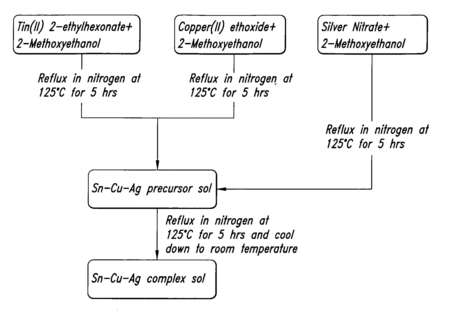
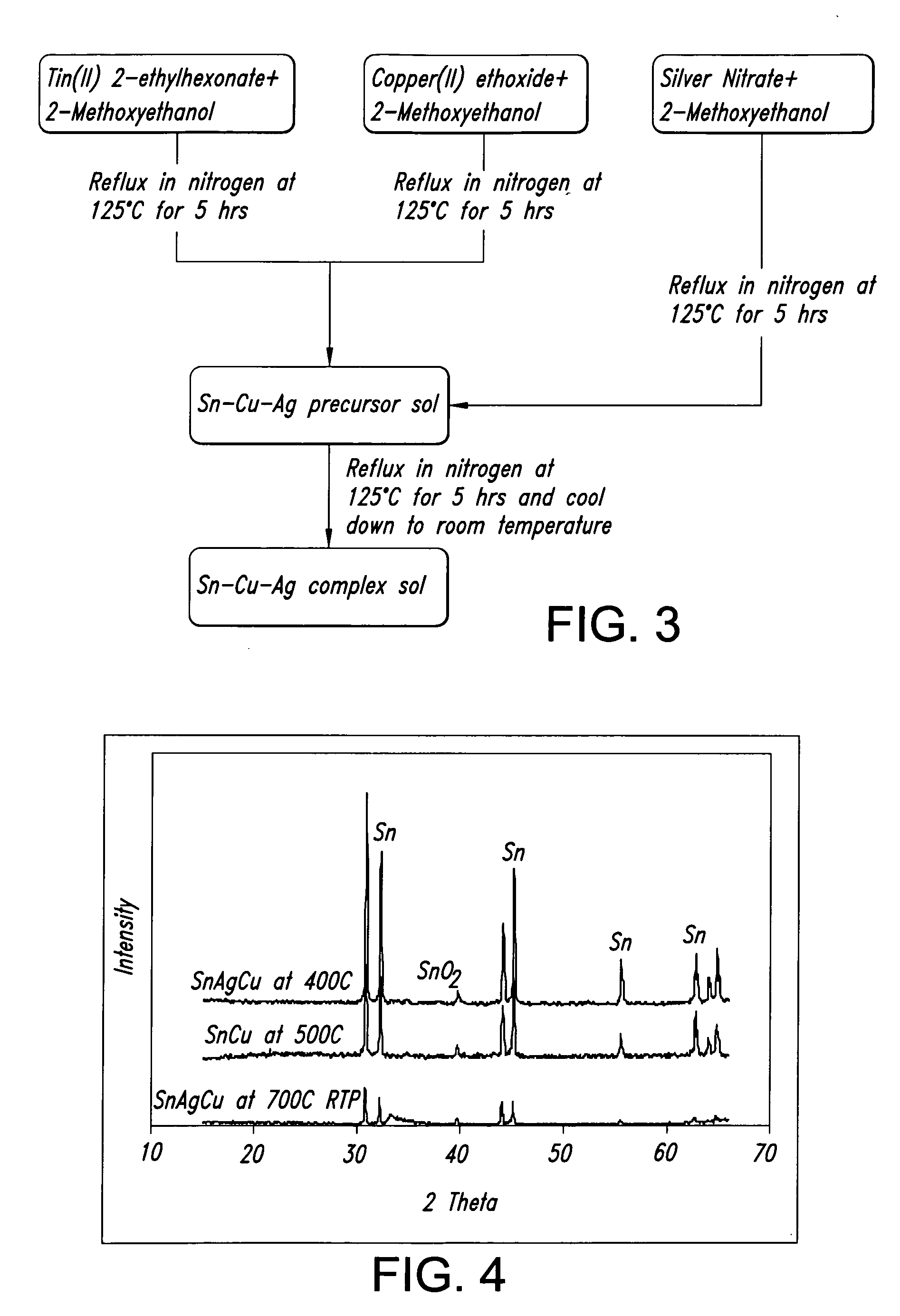
[0048] IC packaging is one of the key enabling technologies for microprocessor performance. As performance increases, the technical challenges increase in the areas of power delivery, heat removal, I / O density, and thermo-mechanical reliability.
[0049] These are the most difficult challenges for improving performance and increasing integration, along with decreasing manufacturing cost.
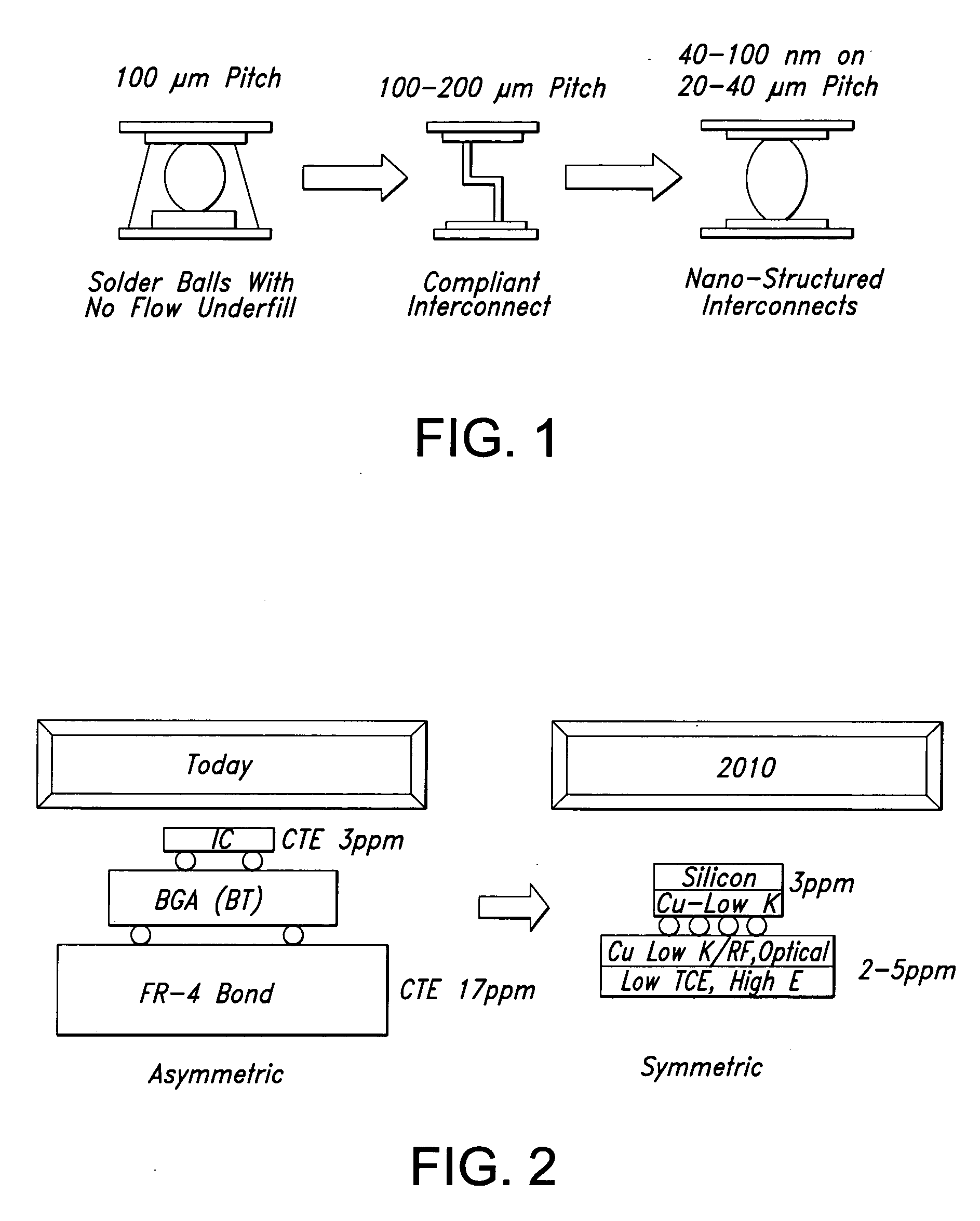
[0050] Decreasing I / O pitch is one of the key technological barriers identified by the 2003 International Technology Roadmap for Semiconductors (ITRS) [1]. See Table 1. The present invention goes beyond the ITRS roadmap in terms of (1) Signal and power integrity (2) I / O connections, and (3) Reworkability. Therefore, the scope of the present invention is not limited by the ITRS roadmap, but goes beyond it by way of a disruptive approach to IC packaging.
TABLE 1ITRS Roadmap for Interconnect Pitch (μm)Year20042007201020132016Wire bond2520202020Area Array Flip Chip1501201009080Peripheral Flip Chip6030202...
PUM
| Property | Measurement | Unit |
|---|---|---|
| Temperature | aaaaa | aaaaa |
| Temperature | aaaaa | aaaaa |
| Length | aaaaa | aaaaa |
Abstract
Description
Claims
Application Information