
Information recording medium and manufacturing process
a technology of information recording medium and manufacturing process, which is applied in the direction of data recording, mechanical record carriers, instruments, etc., can solve the problems of easy shattering, low production efficiency, and poor recording quality, so as to reduce the deviation of position, and improve the effect of recording density
- Summary
- Abstract
- Description
- Claims
- Application Information
AI Technical Summary
Benefits of technology
Problems solved by technology
Method used
Image

Examples
first embodiment
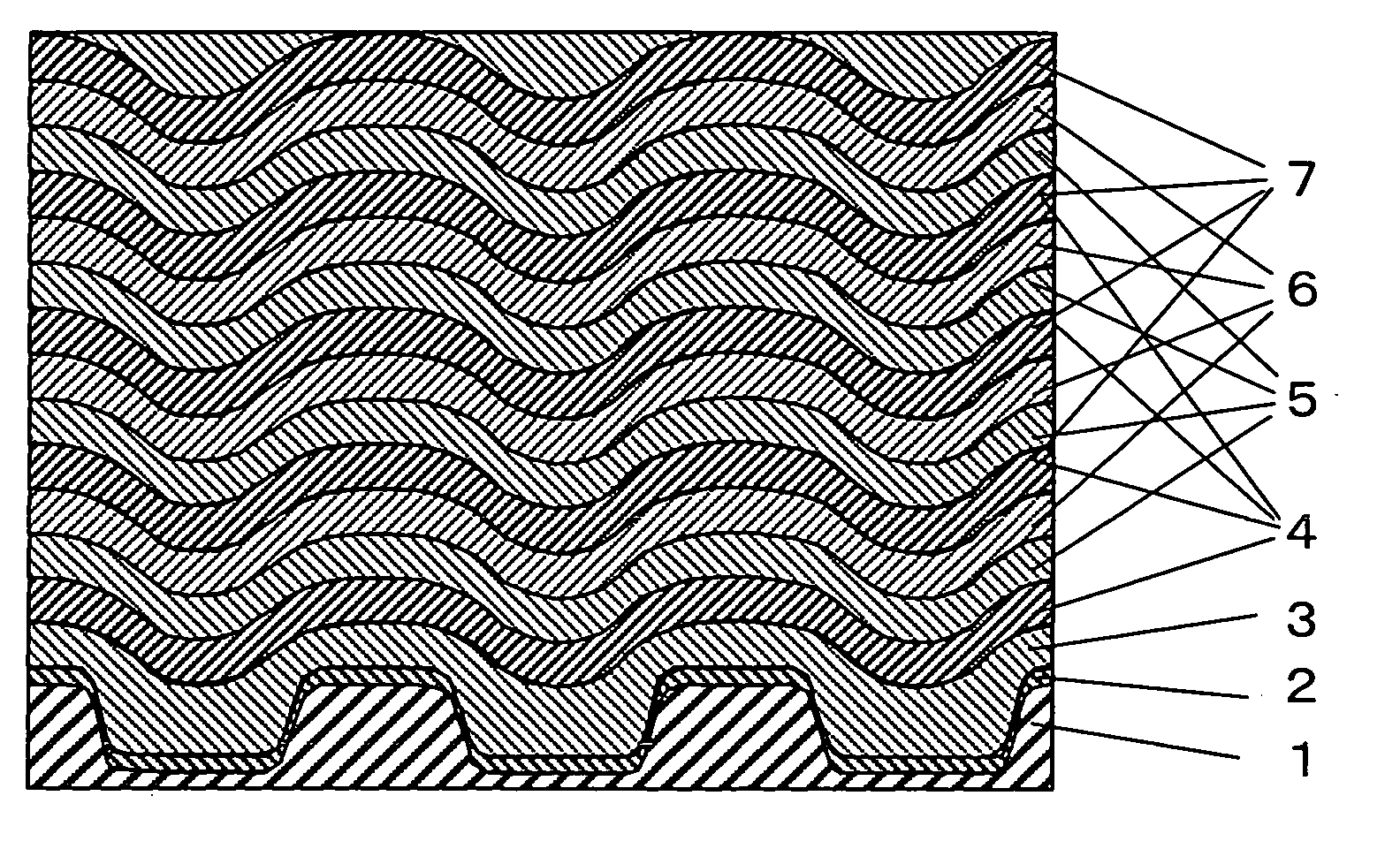
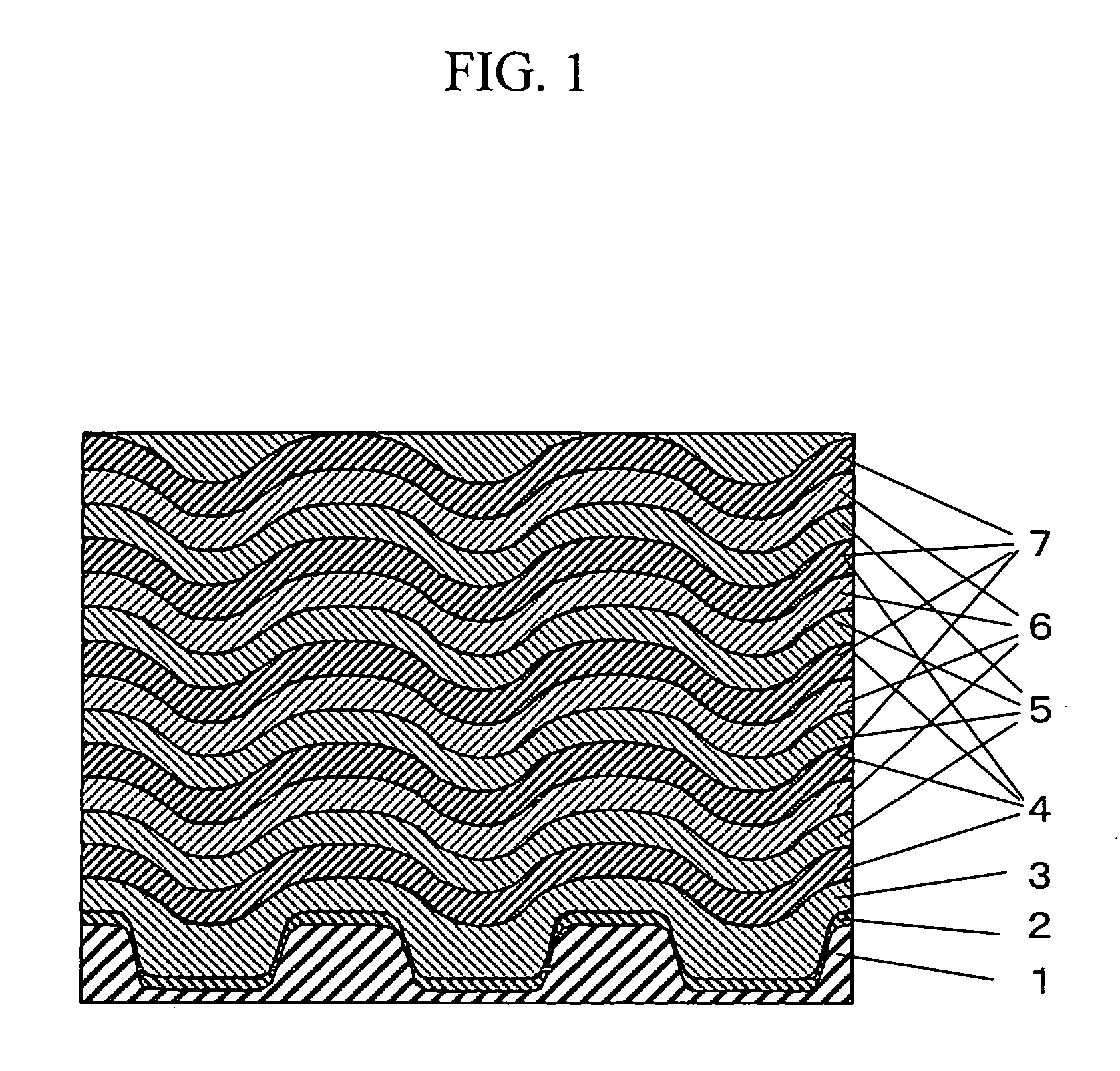
[0110] The specific structure of the recording medium of this invention is described as follows. As shown in FIG. 1, a metallic reflective layer 2 is first of all formed on the substrate 1 including a tracking groove. A dummy layer 3 is next formed, and then the first transparent electrode 4, electrochromic material layer 5, solid electrolyte layer 6, and second transparent electrode 7 films formed in sequence, (from 4 to 7) are repeatedly laminated optically or thermally in two sets or more enclosed by spacers between the transparent electrodes if necessary. Laminating in the sequence of electrochromic material layer 5 and solid electrolyte layer 6 allows a lower drive voltage, however a reverse layer order may also be used. The dummy layer may be a layer of inorganic material formed by bias sputtering described in the second embodiment or even laminated film. The figure shows the case where there is no spacer layer so as can be seen from the figure, an upper section transparent el...
second embodiment
[0181] (Composition, Fabrication Method)
[0182] In the example in the second embodiment, a negative substrate bias voltage is applied and sputtering of inorganic film performed.
[0183] As shown in FIG. 4, an Ag94Pd4Cu2 semitransparent reflective layer 72 with a film thickness of 20 nm was applied to the polycarbonate substrate 71, followed by a dummy layer 73 as a total of three layers of SiO2, GeO2, SiO2 at 400 nm, and then an ITO transparent electrode 74 of 100 nm, an electrochromic material layer 75 of 100 nm, a solid electrolyte layer 76 of 100 nm, an ITO transparent electrode 74 of 100 nm; and followed repeatedly in the same way in the sequence of an electrochromic material layer, ITO transparent electrode, electrochromic material layer, solid electrolyte layer, ITO transparent electrode, electrochromic material layer, solid electrolyte layer, and ITO transparent electrode in five recording layers enclosed on both sides by ITO transparent electrodes. FIG. 4 shows the on-going p...
third embodiment
[0197] The examples in the third embodiment use material other than electrochromic substances, or in other words use multiple laminated layers as the recording layer such as oxidized or sulfurized substances possessing high transmittance.
[0198] (Composition, Fabrication method)
[0199] As shown in FIG. 11, an Ag94Pd4Cu2 semitransparent reflective layer 192 with a film thickness of 20 nm was applied to the polycarbonate substrate 191, followed by a dummy layer 193 as a total of three layers of SiO2, GeO2, SiO2 in a thickness of 400 nm, and then a Te—O—Pd layer of 100 nm thickness as a dummy layer 194, and above this a (ZnS)80(SiO2)20 protective layer 194 of 100 nm thickness, a Te—O—Pd recording layer 195 of 10 nm thickness, a (ZnS)80(SiO2)20 protective layer 196 of 100 nm; and followed repeatedly in the same way by five laminations of recording layers and protective layers. An 0.6 thick mm polycarbonate substrate with an outer diameter of 120 mm thick and an inner diameter of approxi...
PUM
| Property | Measurement | Unit |
|---|---|---|
| size | aaaaa | aaaaa |
| light) transmittance | aaaaa | aaaaa |
| light) transmittance | aaaaa | aaaaa |
Abstract
Description
Claims
Application Information