

Semiconductor device, method of manufacturing the same, and method of evaluating semiconductor device
a semiconductor and semiconductor technology, applied in the direction of semiconductor devices, basic electric elements, electrical appliances, etc., can solve the problems of insufficient measurement of the carrier distribution method, the transistor cannot be produced in volume to be widely used, and the improvement of the performance of the mos transistor by miniaturization is approaching a limit, so as to reduce the thickness of the gate electrode
- Summary
- Abstract
- Description
- Claims
- Application Information
AI Technical Summary
Benefits of technology
Problems solved by technology
Method used
Image

Examples
first embodiment
(1) First Embodiment
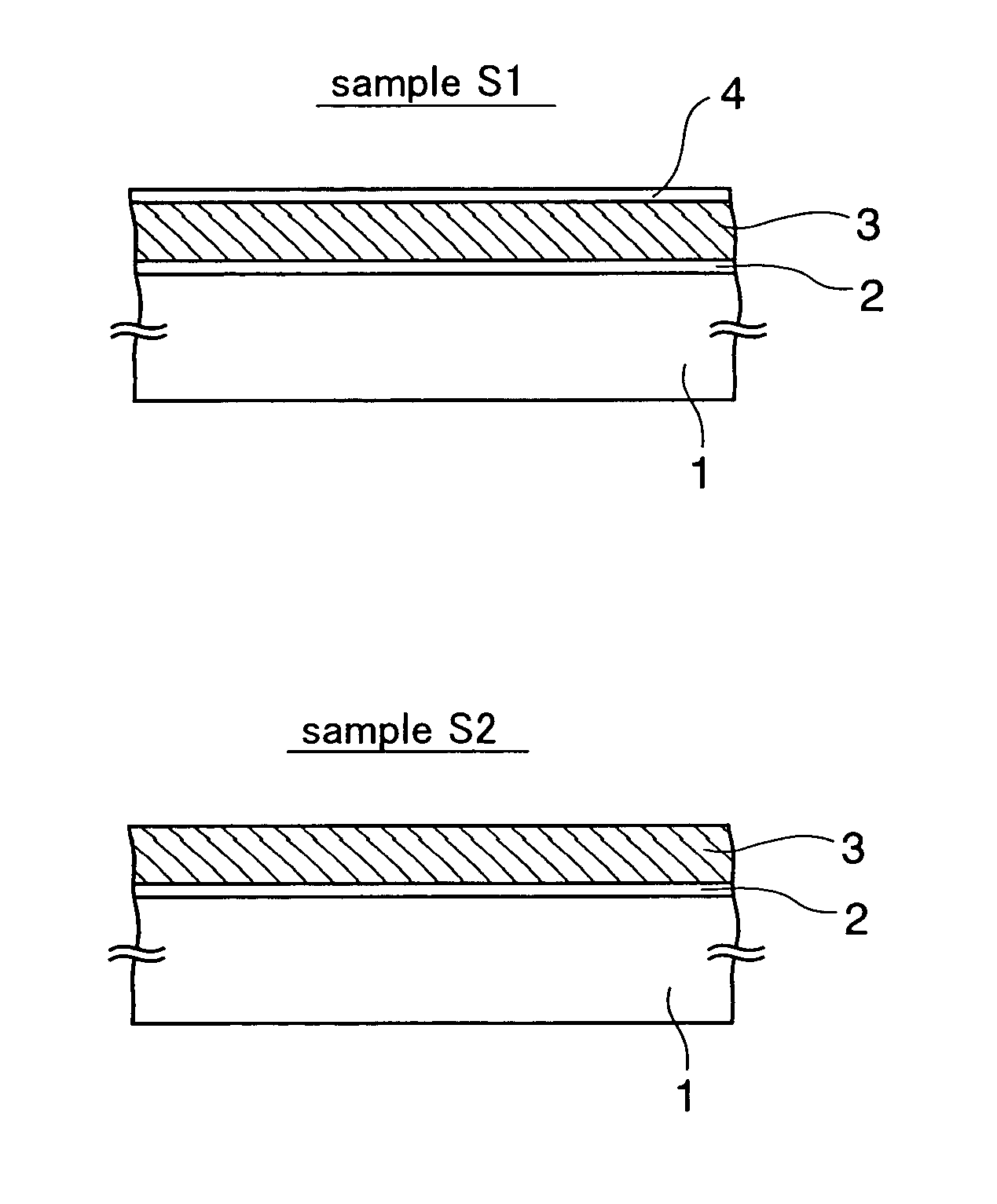
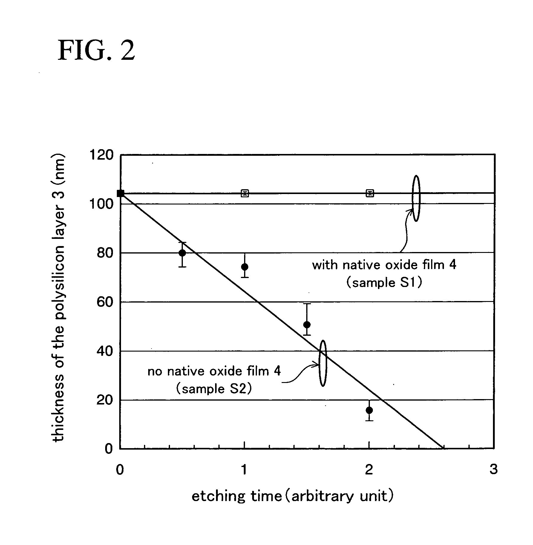
[0054] Recesses of a silicon substrate for growing SiGe layers can be formed by generally-used wet etching in which KOH or a mixture of hydrofluoric acid and nitric acid is used as an etchant. However, use of these etchants makes it difficult to control the shapes of the recesses because the side surface of each recess becomes a gently curved surface as shown in FIG. 1 of Patent Document 1. Accordingly, there is variation in the shapes of the side surfaces of the recesses among elements, and characteristics of MOS transistors may therefore vary among the elements.
[0055] Moreover, if dry etching is used instead of the above-described wet etching, the surfaces of the recesses are damaged by plasma. Accordingly, lattice defects may be created in the SiGe layers epitaxially grown on the recesses.
[0056] In light of these points, the inventor of the present application has searched for an etchant replacing KOH and a mixture of hydrofluoric acid and nitric acid to fin...
second embodiment
(2) Second Embodiment
[0074] Next, a method of fabricating a MOS transistor will be described. In this method, recesses are formed in a silicon substrate by utilizing etching characteristics of a TMAH solution or an organic alkaline solution. The etching characteristics have been revealed in the first embodiment, and SiGe layers in the recesses are used as source / drain electrodes.
[0075]FIGS. 5A to 5G are cross-sectional views of a semiconductor device according to the present embodiment in the process of manufacture.
[0076] To begin with, steps to be performed before the cross-sectional structure shown in FIG. 5A is obtained will be described.
[0077] First, an element isolation trench log for shallow trench isolation (STI) is formed in a p-type silicon (semiconductor) substrate 10 with (001) surface orientation, and then a silicon dioxide layer is buried as an element isolation insulating film 11 in the element isolation trench log. Thereafter, ion implantation is performed on the s...
third embodiment
(3) Third Embodiment
[0117] Next, a method of manufacturing a semiconductor device according to a third embodiment of the present invention will be described.
[0118]FIGS. 8A to 8C are cross-sectional views of a semiconductor device according to the present embodiment in the process of manufacture. Note that the components already described in the second embodiment are denoted by the same reference numerals and codes in these drawings and will not be further described below.
[0119] First, in accordance with the second embodiment, the structure shown in FIG. 5A is completed. However, though ions of p-type impurities have been implanted into the polysilicon layer 14 at a high concentration sufficient to inhibit the etching of polysilicon in the TMAH solution from proceeding in the second embodiment, ions of p-type impurities are implanted into the polysilicon layer 14 at a low concentration at which the polysilicon layer 14 is etched by a TMAH solution partway in the present embodiment....
PUM
 Abstract
Description
Claims
Application Information