Multilayer printed wiring board and a process of producing same
a printing process and wiring board technology, applied in the direction of printing element electric connection formation, insulating substrate metal adhesion improvement, transportation and packaging, etc., can solve the problems of difficult to form a small diameter through hole, difficult to enhance and difficult to form a high-density wiring pattern, etc., to achieve the effect of increasing the density of the wiring pattern
- Summary
- Abstract
- Description
- Claims
- Application Information
AI Technical Summary
Benefits of technology
Problems solved by technology
Method used
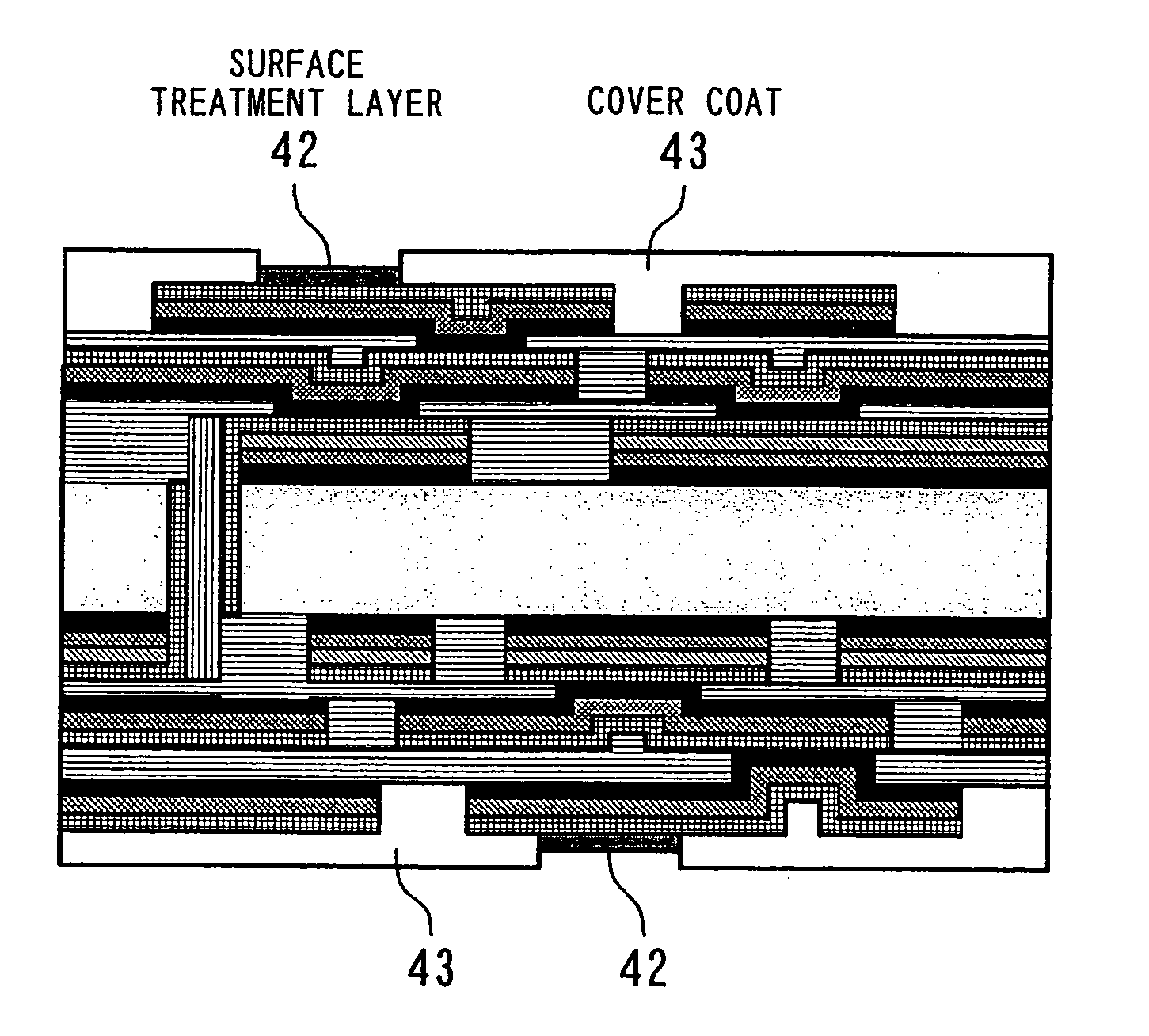
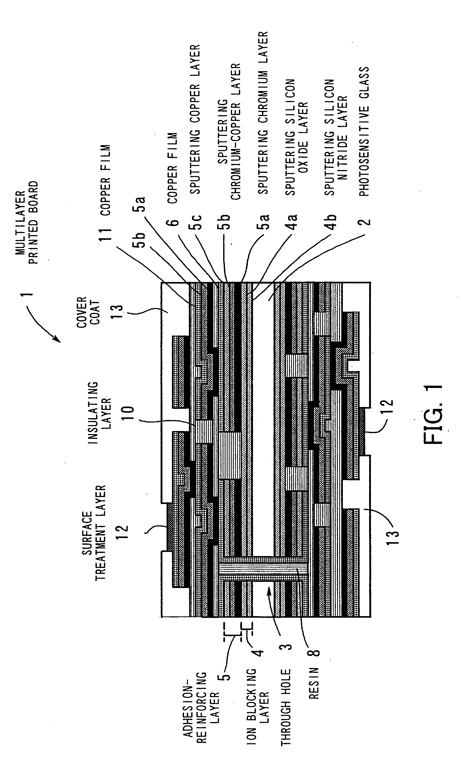
Image

Examples
example 1
[0089] An example according to the first embodiment will be now described.
[0090] In this example, a photosensitive glass (trade name: PEG3, manufactured by HOYA CORPORATION) having the composition stated below was used as the glass substrate.
(wt %)SiO278.0%Li2O10.0%Al2O3 6.0%K2O 4.0%Na2O 1.0%ZnO 1.0%Au0.003% Ag0.08%CeO20.08%
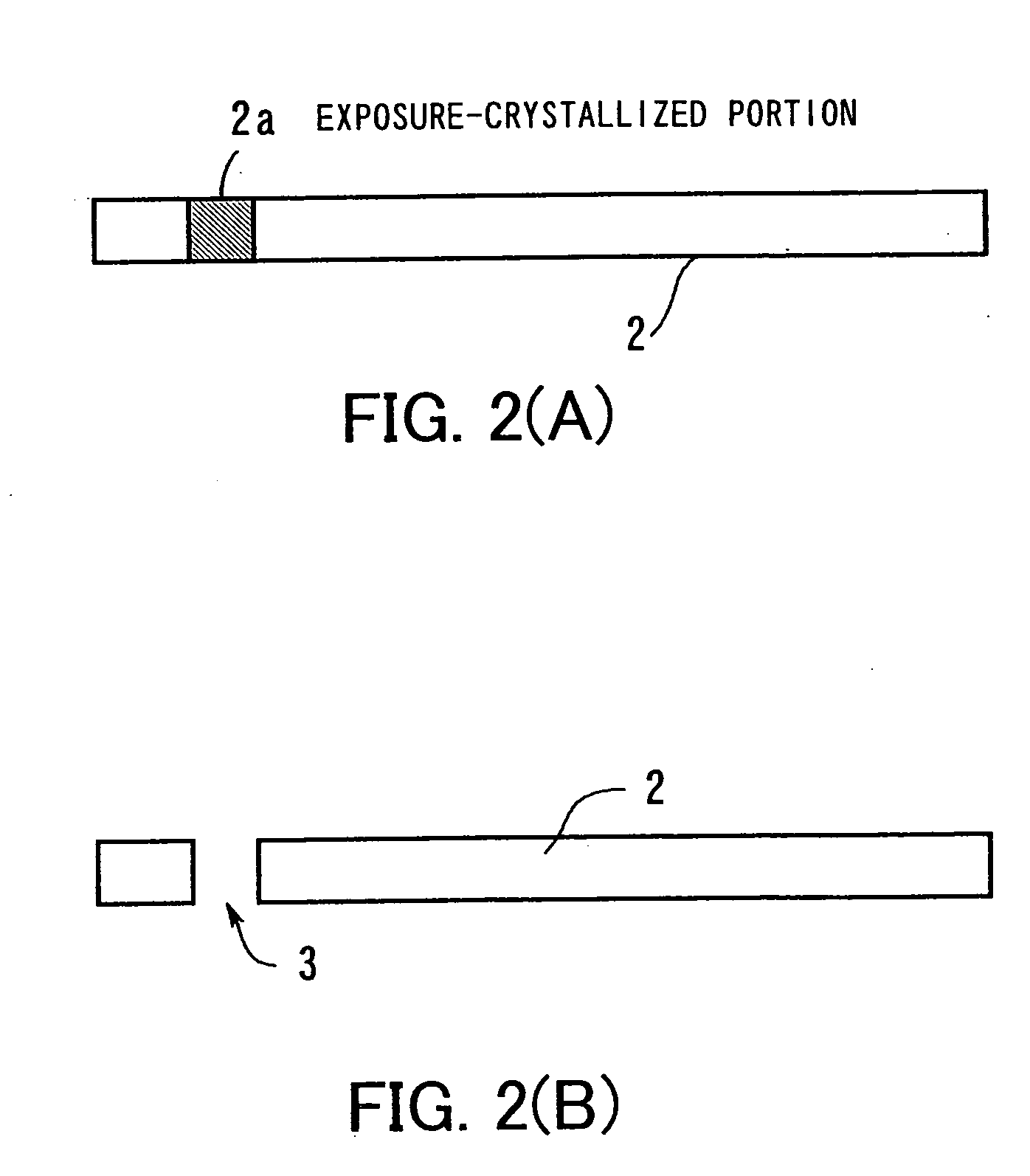
(Through Hole Formation Step)
[0091] 1) With a mask held in close contact with the photosensitive glass, UV light was irradiated onto a through hole portion of the glass through the mask, thereby forming a latent image corresponding to the exposed portion. The mask used was made of silica glass patterned using chromium / chromium oxide. Subsequently, the photosensitive glass was heat-treated at 400° C. to crystallize only the exposed portion.
[0092] 2) Dilute hydrofluoric acid (10% solution) was sprayed on both surfaces of the photosensitive glass to remove the crystallized through hole portion by dissolution, thereby forming a through hole with a diameter φ of...
PUM
| Property | Measurement | Unit |
|---|---|---|
| thickness | aaaaa | aaaaa |
| width | aaaaa | aaaaa |
| diameter | aaaaa | aaaaa |
Abstract
Description
Claims
Application Information