III-V semiconductor nanocrystal complexes and methods of making same

a technology of semiconductor nanocrystals and complexes, which is applied in the field of semiconductor nanocrystal complexes, can solve the problems of limited growth of high-quality iii-v semiconductor nanocrystals, reduced quantum yield, colloidal shell synthesis methods, etc., and achieves high luminescent quantum yield

Active Publication Date: 2006-01-05
SAMSUNG ELECTRONICS CO LTD
View PDF3 Cites 65 Cited by
  • Summary
  • Abstract
  • Description
  • Claims
  • Application Information

AI Technical Summary

Benefits of technology

[0016] In an embodiment, the present invention provides a semiconductor nanocrystal complex comprising a III-V semiconductor nanocrystal core, wherein the semiconductor nanocrystal complex is stable and exhibits a high luminescent quantum yield.
[0017] Additionally, the present invention provides for a method of making a semiconductor nanocrystal complex comprising a III-V semiconductor nanocrystal core, wherein the semiconductor nanocrystal complex is stable and exhibits a high luminescent quantum yield.

Problems solved by technology

Because the nanocrystal may have a large surface area to volume ratio, dislocations present on the surface or adsorbed surface molecules having a significant potential difference from the nanocrystal itself will tend to trap excited state carriers and prevent radiactive recombination and thus reduce quantum yield.
One exemplary problem associated with known colloidal shell synthesis methods is that they are limited in regard to the growth of high quality III-V semiconductor nanocrystals due, at least in part, to the covalent nature of the material.
Additionally, the growth of III-V nanocrystals is difficult because of the need for vacuum growth and strict humidity conditions.
Etching has shown to improve the quantum yield of III-V materials however, the etching process introduces problems when bonding ligands to the surface of the nanocrystals.
This causes poor colloidal stability and makes the complexes incompatible for a variety of applications.
In addition, the etched surface does not provide sufficient electronic passivation.
As a result, electronic interaction between a matrix material and the nanocrystal may result in fluorescence quenching.
This is not conducive to the scale up and production of large quantities of IlI-V semiconductor nanocrystal complexes.
By readily losing their fluorescence, these quantum dot materials are simply unsuitable for most applications.

Method used


Image

  • III-V semiconductor nanocrystal complexes and methods of making same
  • III-V semiconductor nanocrystal complexes and methods of making same
  • III-V semiconductor nanocrystal complexes and methods of making same

Examples


example

Preparing a III-V Semiconductor Nanocrystal Complex

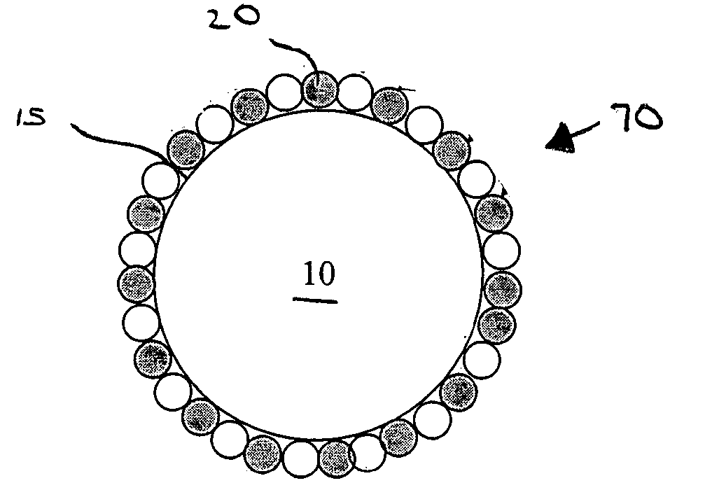
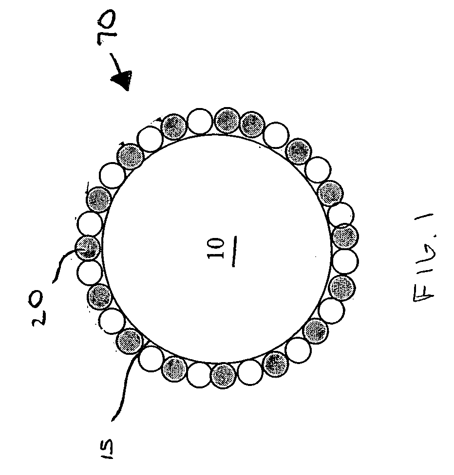
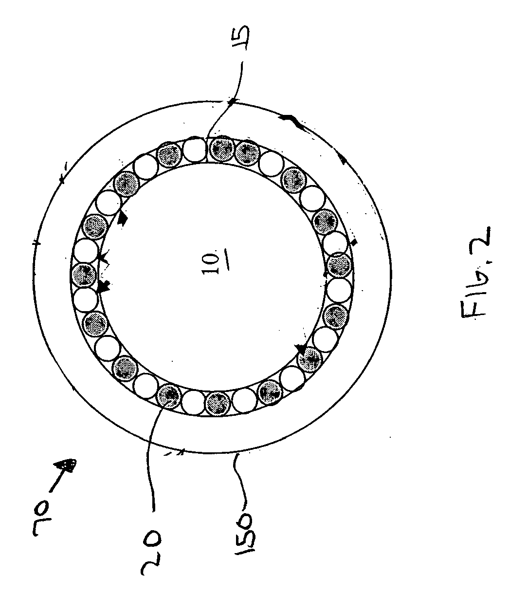
[0041] The present example discloses how to prepare a stable, high luminescent quantum yield semiconductor nanocrystal complex comprising an InGaP semiconductor nanocrystal core and a Zn metal layer formed on the outer surface of the semiconductor nanocrystal core after synthesis of the semiconductor nanocrystal core.

[0042] First, an indium precursor is prepared. In a reaction flask, 292 g / mol of 0.9 Molar indium (III) acetate (99.99% pure), is added to 367 g / mol of 0.1 Molar gallium acetylacetonoate (99% pure) and 256.4 g / mol of 3 Molar almitic acid (99% pure). The ingredients are mixed and heated to 130° C. for 2 hours under vacuum. The vacuum removes the acetic acid that could form. The resulting solution should be clear but may have a yellow tint.

[0043] Next, a phosphorous precursor and a zinc oleate precursor is prepared. The phosphorous precursor is formed by adding 0.3 mL TMSphosphine and 4.0 mL TOP under nitrogen. The zin...


PUM

PropertyMeasurementUnit
diameteraaaaaaaaaa
diameteraaaaaaaaaa
mean diameteraaaaaaaaaa

Abstract

A semiconductor nanocrystal complex that is stable and has high luminescent quantum yield. The semiconductor nanocrystal complex has a semiconductor nanocrystal core of a III-V semiconductor nanocrystal material. A method of making a semiconductor nanocrystal complex is also provided. The method includes synthesizing a semiconductor nanocrystal core of a III-V semiconductor nanocrystal material, and forming a metal layer on the semiconductor nanocrystal core after synthesis of the semiconductor nanocrystal core.

Description

CROSS-REFERENCE TO RELATED APPLICATIONS [0001] The present application claims priority to U.S. Provisional Application No. 60 / 569,452, filed May 10, 2004, which is incorporated by reference herein.FIELD OF THE INVENTION [0002] The present invention relates to semiconductor nanocrystal complexes and particularly to III-V semiconductor nanocrystal complexes. The present invention also relates to methods of making semiconductor nanocrystal complexes. BACKGROUND OF THE INVENTION [0003] Semiconductor nanocrystals are typically tiny crystals of II-VI, III-V, IV-VI materials that have a diameter between 1 nanometer (nm) and 20 nm. In the strong confinement limit, the physical diameter of the nanocrystal is smaller than the bulk excitation Bohr radius causing quantum confinement effects to predominate. In this regime, the nanocrystal is a 0-dimensional system that has both quantized density and energy of electronic states where the actual energy and energy differences between electronic sta...

Claims


Application Information

Patent Timeline
Patent Type & Authority Applications(United States)
IPC IPC(8): H01L31/00H01L21/00C01B19/00C30B7/00C30B29/60
CPCB82Y20/00Y10S977/821C01G9/08C01G11/02C01G13/00C01G21/21C01G25/00C01P2004/64C01P2006/40C09K11/02C09K11/025C09K11/565C09K11/62C09K11/661C09K11/70C09K11/7492C09K11/75C09K11/88C09K11/883C09K11/892C23C18/00C23C18/1204C23C18/1295C30B7/00C30B29/605C30B33/00B82Y30/00Y10S977/817Y10T428/12528Y10T428/2982Y10T428/12535Y10T428/2991Y10T428/1266Y10T428/12785Y10S977/773Y10S977/834Y10S977/774Y10S977/815Y10S977/813Y10S977/818Y10S977/819Y10S977/816Y10S977/82Y10S977/822Y10S977/823
Inventor LIU, WEIPENG, ADAMLANDRY, DANIEL
Owner SAMSUNG ELECTRONICS CO LTD
Why Eureka
Try Eureka