Illumination system optimized for throughput and manufacturability

a technology of illumination system and throughput, applied in the field of imaging system, can solve the problems of increasing the cost of the illumination system, and achieve the effect of increasing the ratio of the area of the recycling mirror, increasing the recycling efficiency, and fast construction

Inactive Publication Date: 2006-01-05
ANVIK CORP
View PDF1 Cites 11 Cited by
  • Summary
  • Abstract
  • Description
  • Claims
  • Application Information

AI Technical Summary

Benefits of technology

[0023] An advantage of the invention is additional recycling efficiency gained by making the recycling segment larger in diameter than the homogenizer segments, thus increasing the ratio of the area of the recycling mirror to the homogenizer input aperture.
[0024] Another advantage of the invention is that the standardized design of the segments allows illumination systems quickly to be constructed using a selected number of extension segments, saving the cost and time required to develop and fabricate designs customized for specific lengths and for specific condenser lens assemblies.
[0025] Still another advantage of the invention is additional system efficiency gained by increasing homogenizer efficiency so more energy reaches the image plane, which allows greater lithography system throughput in a production environment.

Problems solved by technology

The first approach, increased homogenizer length, increases cost of the illumination system.

Method used


Image

  • Illumination system optimized for throughput and manufacturability
  • Illumination system optimized for throughput and manufacturability
  • Illumination system optimized for throughput and manufacturability

Examples


Embodiment Construction

Homogenizer with Energy Recycling

[0038] The high-efficiency energy-recycling system is schematically illustrated in FIG. 11 as part of an illumination system optimized for resist exposure, photoablation, or crystallization. The patterning mask 10 and substrate 12 are rigidly held on a planar scanning stage 14. A projection lens 16, in conjunction with a fold mirror 18 and reversing unit 20, forms the image of a portion of the mask 10 on the substrate 12. The stage 14 is scanned in a serpentine fashion, imaging the entire mask pattern onto the substrate 12.

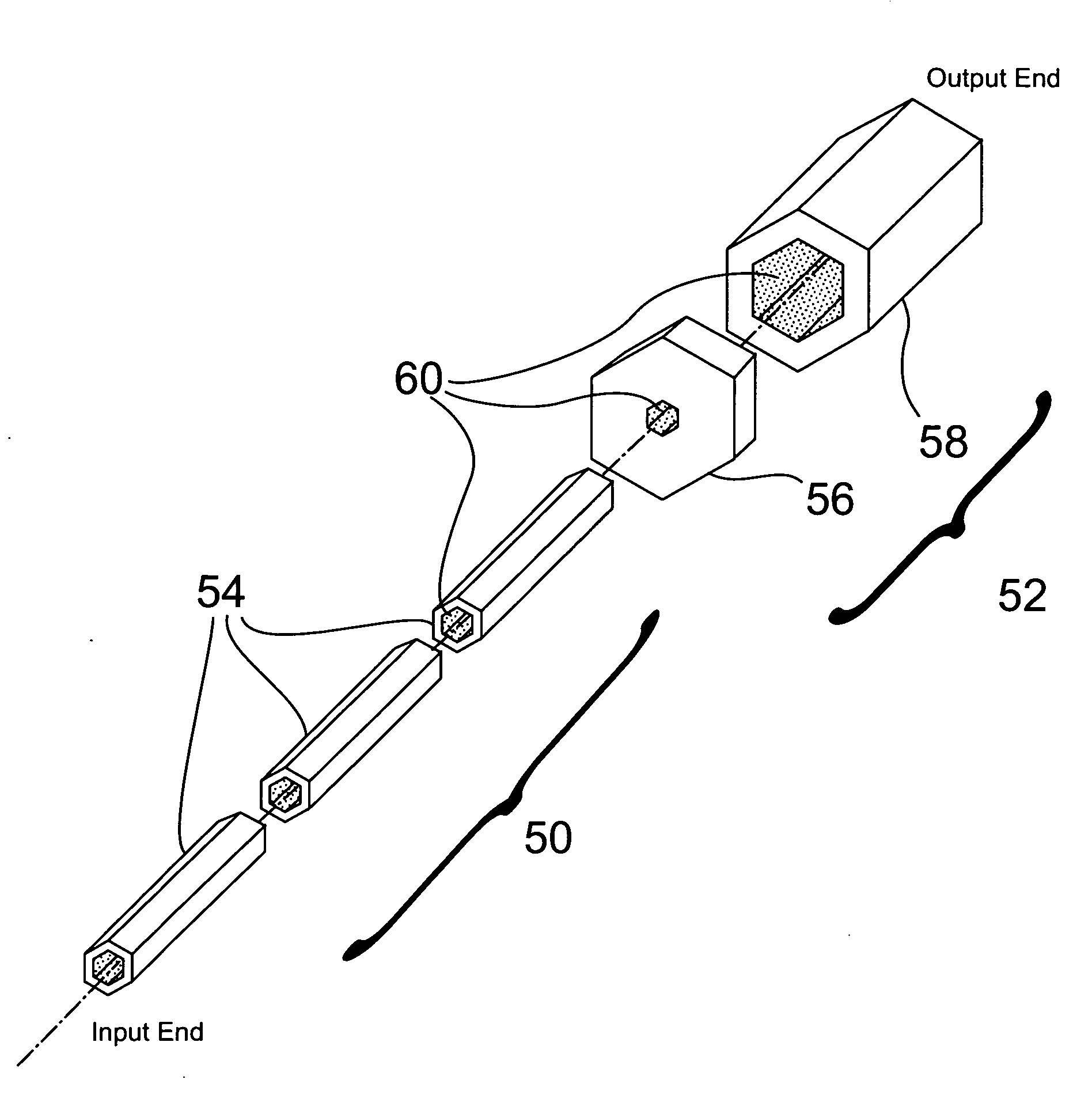
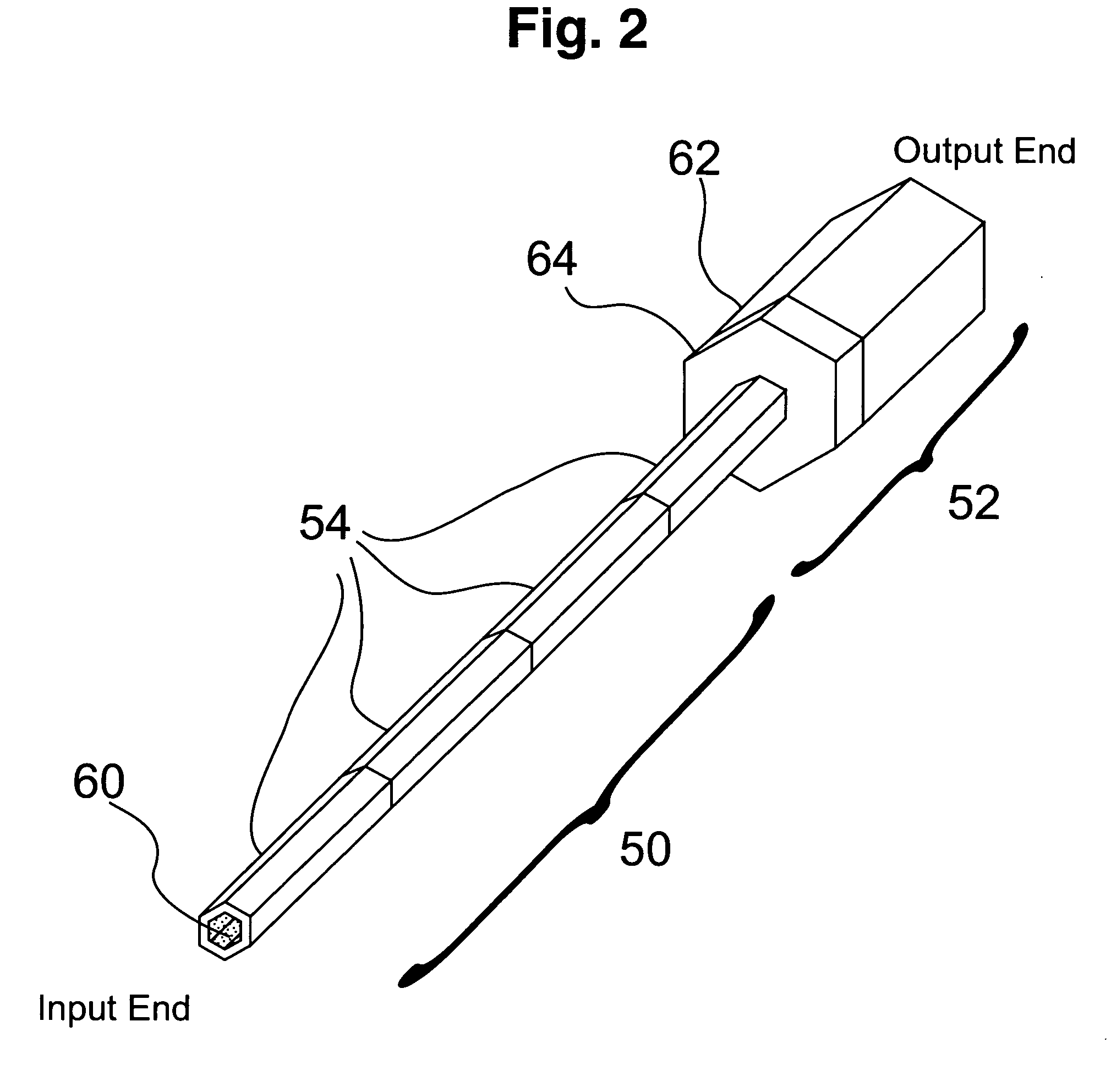
[0039] A laser 22 provides the illumination for exposure. A lens system (26 and 28) shapes the output beam 24 of the laser, which is focused into the homogenizer 34. The homogenizer 34, which has a hexagonal cross-section, uniformizes the input beam, producing a hexagonal self-luminous radiation source at the output plane. A condenser lens assembly, comprising elements 40 and 42, images the output plane of the homogenizer 34 ont...


PUM


Abstract

An optimized illumination system that efficiently produces uniform illumination for exposure, photoablation, and laser crystallization systems. The illumination system includes a homogenizer that uniformizes and shapes a light beam, which is directed onto a mask by condenser optics. The illumination system recycles radiation by directing light reflected by the mask back into the illumination system, where an apertured mirror situated at the input end re-directs it back toward the mask. The relative areas of the mirror and aperture affect recycling efficiency and system throughput, so the system features a larger-diameter recycling segment enabling greater mirror-to-aperture area ratios. An added segment at the output end of the homogenizer matches the homogenizer diameter to the projection imaging system object field size. This standardizes the homogenizer and condenser lens integration, reducing the need for customized parts and thus reducing manufacturing time and expense.

Description

CROSS-REFERENCE TO RELATED APPLICATION [0001] Not applicable. STATEMENT REGARDING FEDERALLY SPONSORED RESEARCH OR DEVELOPMENT [0002] Not applicable. BACKGROUND OF THE INVENTION [0003] 1. Field of the Invention [0004] This invention relates to imaging systems for creating desired radiation patterns on radiation-sensitive surfaces such as substrates used in microelectronics circuits and boards, and more particularly relates to homogenizer systems, which provide radiation of uniform intensity for the imaging system, ensuring uniform radiation dosage and high efficiency, allowing for high-speed manufacturing. [0005] 2. Description of Related Art [0006] Large-area lithographic exposure systems are required as production tools for the manufacturing of numerous products, including multi-chip modules for high-density electronic packaging, flat-panel displays, printed circuit boards, and semiconductor integrated circuits. Many types of exposure systems are used in the industry, including con...

Claims


Application Information

Patent Timeline
Patent Type & Authority Applications(United States)
IPC IPC(8): G03B27/00
CPCG02B27/0927G03F7/70075G02B27/0994
Inventor RAGHUNANDAN, SHYAMJAIN, KANTIZEMEL, MARC I.KLOSNER, MARC A.KUCHIBHOTLA, SIVARAMA K.
Owner ANVIK CORP
Why Eureka
Try Eureka