

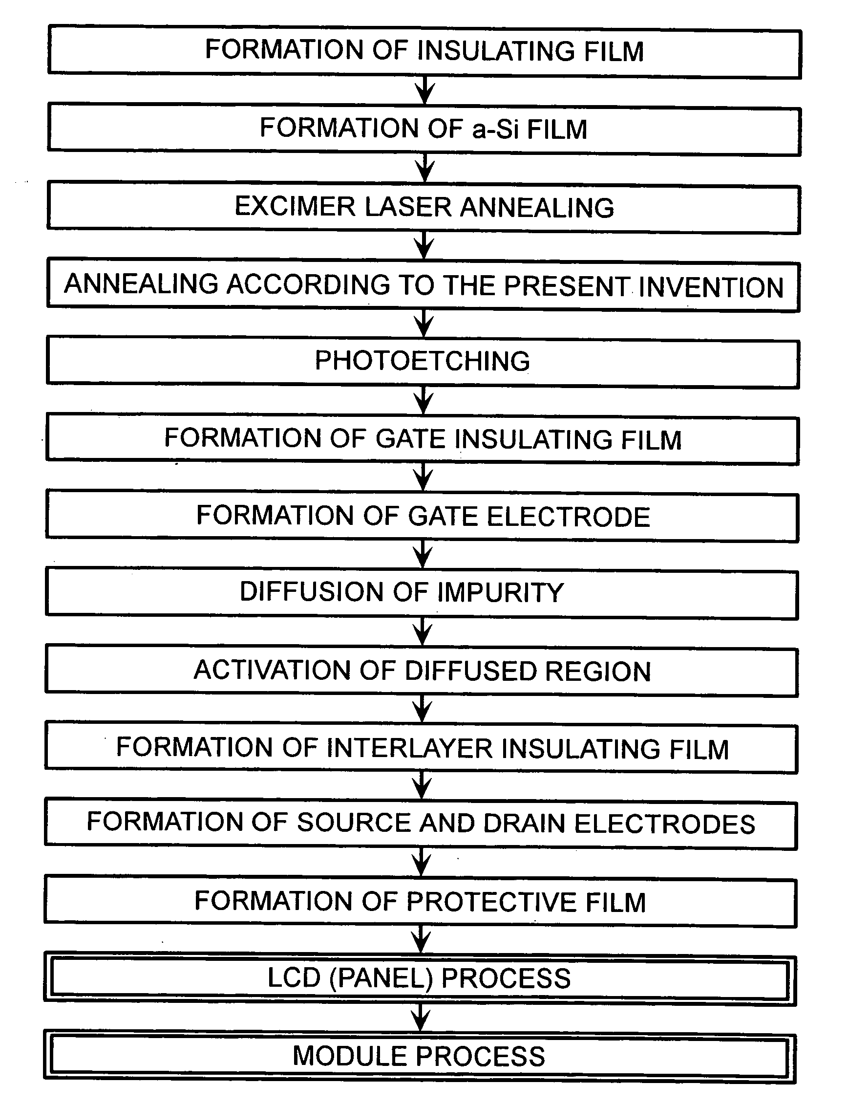
Method of manufacturing display device
a display device and laser annealing technology, applied in the direction of manufacturing tools, identification means, instruments, etc., can solve the problems of insufficient capacity for application as a driver circuit or the like for driving a liquid crystal panel, pulse duration and a change in output in terms of time, and achieve the effect of reducing or eliminating the influence of interference on the laser-irradiated area
- Summary
- Abstract
- Description
- Claims
- Application Information
AI Technical Summary
Benefits of technology
Problems solved by technology
Method used
Image

Examples
Embodiment Construction
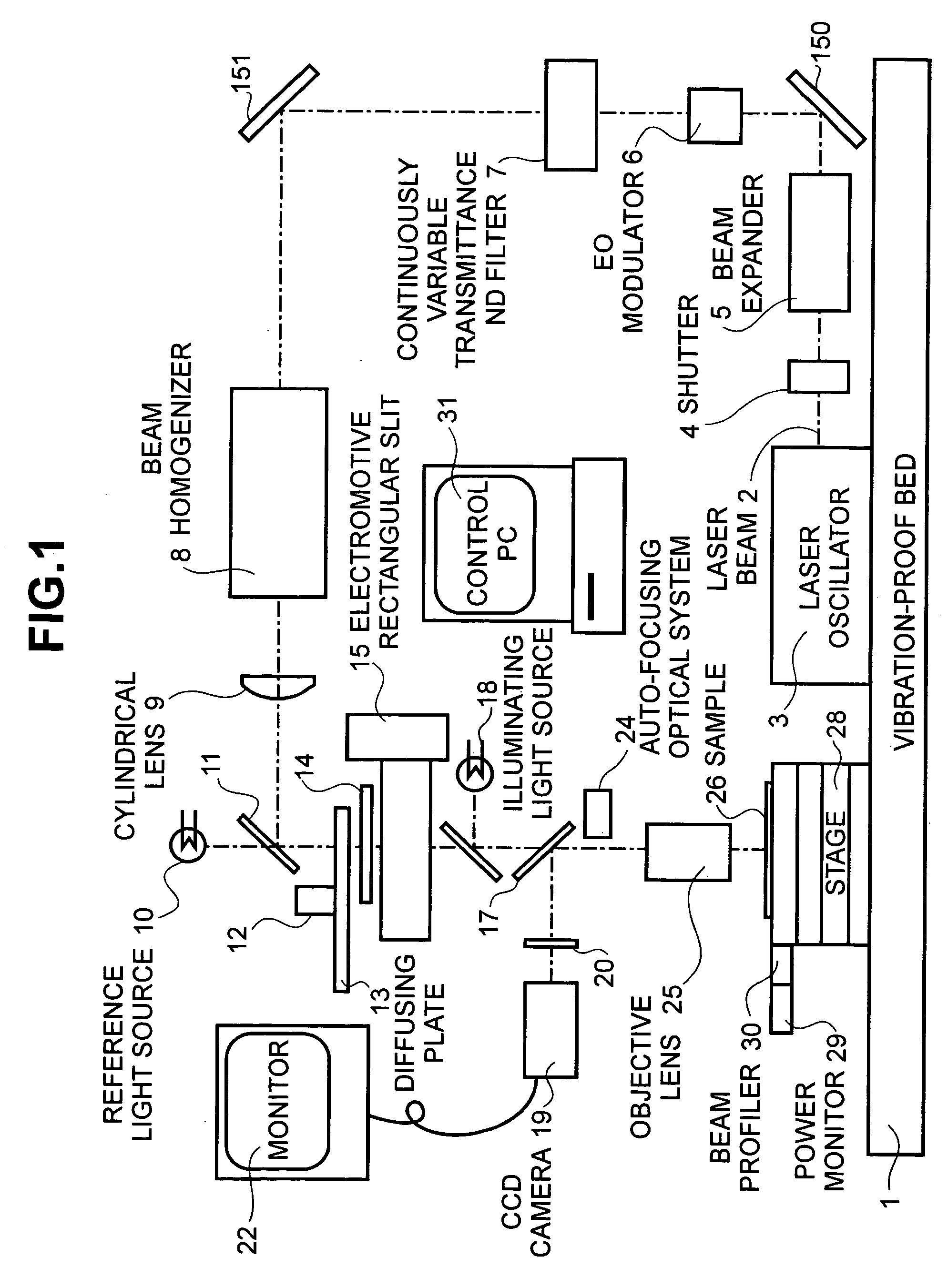
[0045] A detailed explanation of the present invention will be presented with reference to the drawings. FIG. 1 is a diagram showing the constitution of the laser annealing apparatus relating to the first embodiment of the present invention, the base of which is constituted by a bed 1, which is provided with a vibration proofing mechanism (not shown). The bed 1 serves as a support for a laser oscillator 3 for emitting a continuous wave laser beam 2, a shutter 4 for turning the laser beam 2 on and off, a beam expander 5 for expanding the beam diameter of the laser beam 2 that is output from the laser oscillator 3, an electro-optical modulator. (hereinafter “EO modulator”) 6 for effecting a pulsing and temporal modulation of the energy of the laser beam 2, a continuously variable transmittance ND filter 7 for regulating the energy of the laser beam 2, a beam-homogenizer 8 for giving the laser beam 2 a uniform energy distribution, and a cylindrical lens 9 for compressing the laser beam...
PUM
| Property | Measurement | Unit |
|---|---|---|
| crystal grain sizes | aaaaa | aaaaa |
| crystal grain sizes | aaaaa | aaaaa |
| diameter | aaaaa | aaaaa |
Abstract
Description
Claims
Application Information