Low temperature process for polysilazane oxidation/densification

a polysilazane and low temperature technology, applied in the direction of superimposed coating process, resistive material coating, liquid/solution decomposition chemical coating, etc., can solve the problems of difficult to form void-free or seam-free gaps using standard cvd or pecvd techniques, difficult to fill narrow features such as narrow features, and electrically leak films, etc., to achieve high oxygen content, low cost, and easy processing

Active Publication Date: 2006-01-05
MICRON TECH INC
View PDF32 Cites 107 Cited by
  • Summary
  • Abstract
  • Description
  • Claims
  • Application Information

AI Technical Summary

Benefits of technology

[0015] The present silicon oxide material is useful for filling narrow gaps in a PMD interlayer and for filling trenches in shallow trench isolation structures. PMD interlayers may include polysilicon gates and a barrier layer on a substrate, with narrow gaps between the gate structures. The material of the invention can be deposited and processed to fill spaces between the structures with a silicon oxide insulating fill. The process in accordance with the invention achieves a solid, void-free silicon oxide fill or layer having a high oxygen content that can be easily processed and will maintain its integrity in subsequent processing steps.
[0016] Advantages of the present procedure include low cost, simplicity, batch processing, and a low thermal budget, among others. The procedure can be used for the oxidation and densification of polysilazane films and spin-on-dielectric (SOD) films having a lower oxygen content than silicon dioxide (SiO2) or hydroxyl content to produce a film that has improved uniform etch properties. The low temperature process (T<100° C.) is particularly useful for deep trench applications (1000-3000 Å or greater) in the fabrication of Flash memory, FINFET, RAD, SDRAM, PC-RAM, and dense DRAM structures. The process avoids the use of high temperatures (i.e., 700-800° C.), which can damage other features that are present on the substrate.

Problems solved by technology

Such trenches can have a width as narrow as 0.01 to 0.05 microns (μm) or smaller, and filling such narrow features can be difficult.
With high aspect ratio features, the width becomes narrower while the depth becomes much greater, it is difficult to form a void-free or seam-free gap fill using standard CVD or PECVD techniques.
High temperature processing after formation of an oxide insulating layer such as an annealing or high temperature densification step can cause a loss of oxygen from the dielectric material resulting in electrically leaking films.
Although demonstrating good filling properties, such a process is slow and not cost effective.
A silicon oxide film is formed by spin-coating a liquid solution of the silicon-containing polymer onto a surface of a substrate, baking the material to remove the solvent, and then thermally oxidizing the polymer layer in an oxygen, or steam, atmosphere at an elevated temperature of up to about 1000° C. A drawback is that high temperature treatments can degrade other structures such as aluminum or other metal wiring layer that have a low thermal tolerance.
Another drawback of current methods is the high cost and time required for processing.
Such products may require limited thermal budget processing where extensive densification can hurt device parameters.

Method used


Image

  • Low temperature process for polysilazane oxidation/densification
  • Low temperature process for polysilazane oxidation/densification
  • Low temperature process for polysilazane oxidation/densification

Examples


Embodiment Construction

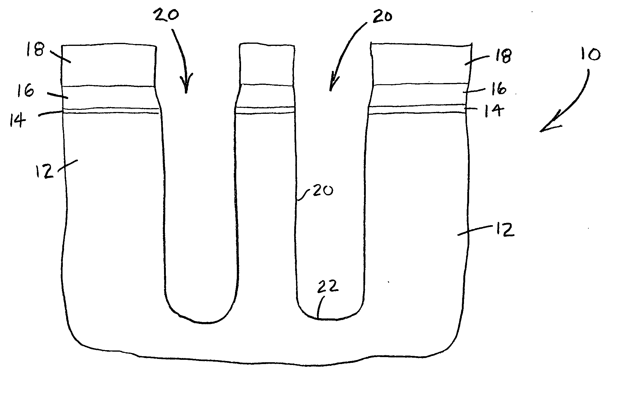
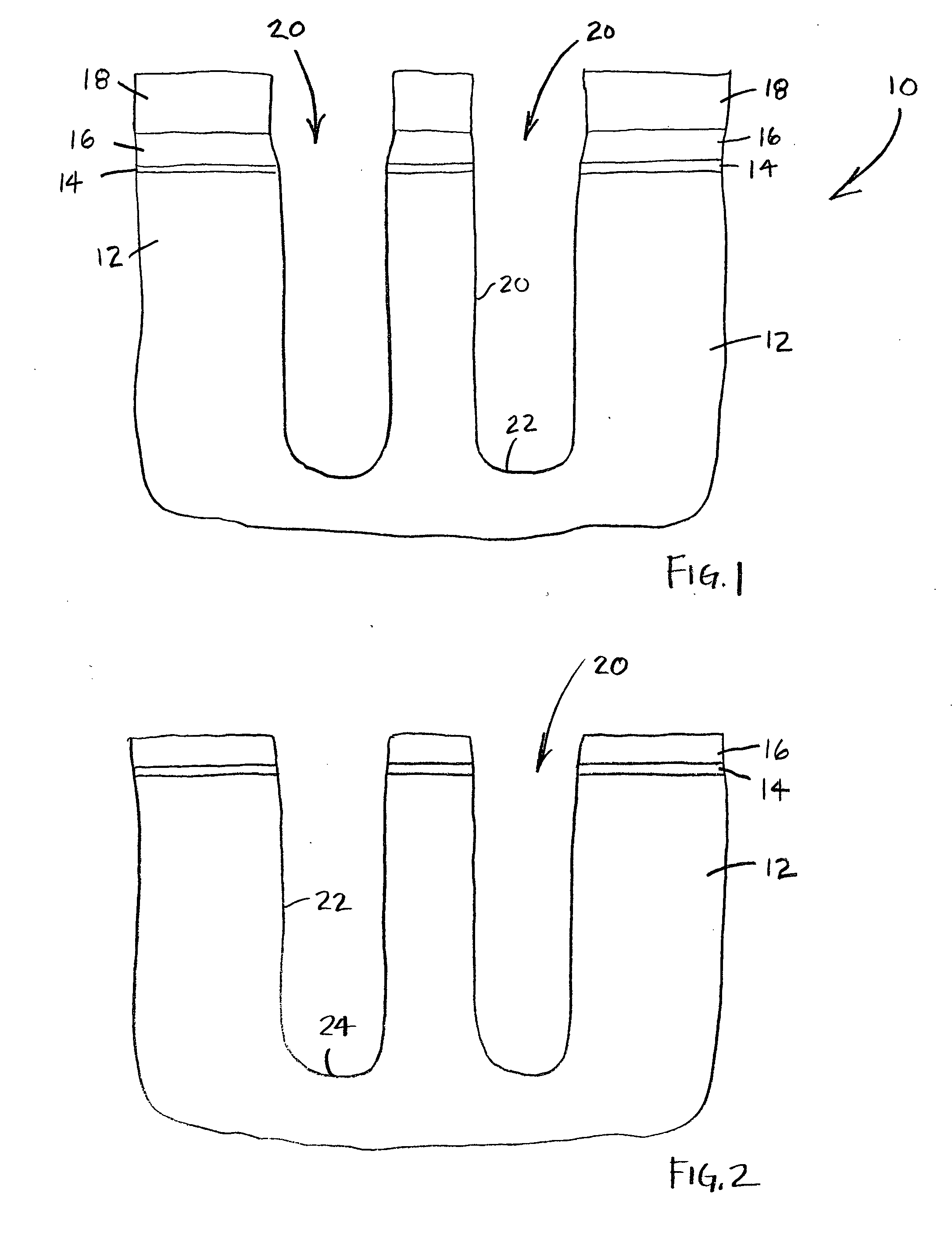
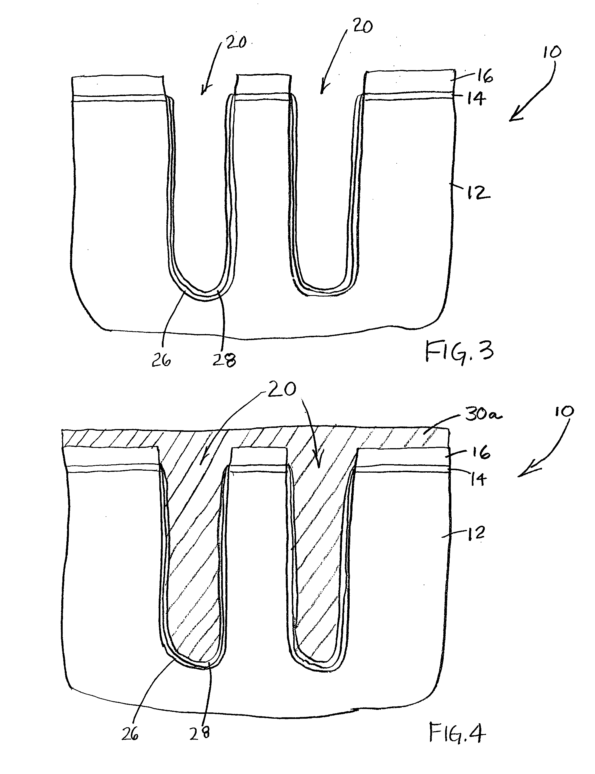
[0029] The invention will be described generally with reference to the drawings for the purpose of illustrating the present preferred embodiments only and not for purposes of limiting the same. The figures illustrate processing steps for use in the fabrication of semiconductor devices in accordance with the present invention. It should be readily apparent that the processing steps are only a portion of the entire fabrication process.

[0030] In the context of the current application, the term “semiconductor substrate” or “semiconductive substrate” or “semiconductive wafer fragment” or “wafer fragment” or “wafer” will be understood to mean any construction comprising semiconductor material, including but not limited to bulk semiconductive materials such as a semiconductor wafer (either alone or in assemblies comprising other materials thereon), and semiconductive material layers (either alone or in assemblies comprising other materials). The term “substrate” refers to any supporting s...


PUM

PropertyMeasurementUnit
temperatureaaaaaaaaaa
thicknessaaaaaaaaaa
thicknessaaaaaaaaaa

Abstract

Semiconductor devices, structures and systems that utilize a polysilazane-based silicon oxide layer or fill, and methods of making the oxide layer are disclosed. In one embodiment, a polysilazane solution is deposited on a substrate and processed with ozone in a wet oxidation at low temperature to chemically modify the polysilazane material to a silicon oxide layer.

Description

FIELD OF THE INVENTION [0001] The invention relates generally to semiconductor processing methods of forming and utilizing insulative materials for electrical isolation in integrated circuits, and more particularly to processes for forming insulating films from polysilazane coatings. BACKGROUND OF THE INVENTION [0002] In the fabrication of semiconductor integrated circuits, semiconductor elements are integrated and laid out within a small area on a chip requiring the devices to be placed in close proximity to each other. With the continuing decrease in the dimensions and spacing of devices on integrated circuits (ICs), insulative materials are deposited to electrically isolate the various active components such as transistors, resistors and capacitors. Isolation insulative materials are typically made of silicon dioxide (SiO2). [0003] For example, interlayer dielectric (ILD) or pre-metal dielectric (PMD) layers isolate structures from metal interconnect layers, which may require fil...

Claims


Application Information

Patent Timeline
Patent Type & Authority Applications(United States)
IPC IPC(8): H01L21/469H01L21/31
CPCH01L21/3125H01L21/316H01L21/76205H01L21/76801H01L21/76832H01L21/76826H01L21/76828H01L21/76829H01L21/76831H01L21/76802H01L21/02222H01L21/02282H01L21/02164H01L21/02236H01L21/02343
Inventor FUCSKO, JANOSSMYTHE, JOHN A. IIILI, LIWALDO, GRADY S.
Owner MICRON TECH INC
Why Eureka
Try Eureka