Method of forming a layer and forming a capacitor of a semiconductor device having the same layer

a semiconductor device and capacitor technology, applied in the field of methods of forming a layer and forming a semiconductor capacitor having the layer, can solve the problems of deteriorating the characteristics of a semiconductor device, loading effect of the semiconductor device, and conventional chemical vapor deposition process, etc., to achieve excellent insulation properties, reduce leakage current, and low hydrogen content

Inactive Publication Date: 2006-01-19
SAMSUNG ELECTRONICS CO LTD
View PDF17 Cites 436 Cited by
  • Summary
  • Abstract
  • Description
  • Claims
  • Application Information

AI Technical Summary

Benefits of technology

[0034] According to an embodiment of the present invention, an adsorption layer formed using a first reactant or a layer formed by reacting reactants in the adsorption layer with a second reactant may be treated with nitrogen (N2) plasma. Therefore, hydrogen bonds of the adsorption layer or the layer may be removed. Thus, the layer may have low hydrogen content. In addition, the plasma for removing impurities is applied to a layer formed by an ALD process. Therefore, the impurities in the layer may be effectively removed to reduce leakage current from the layer and to form the layer having excellent insulation property. Furthermore, when the layer is employed for a dielectric layer of a capacitor, the capacitor may have improved electrical characteristics and enhanced reliability.

Problems solved by technology

Conventional chemical vapor deposition (CVD) processes, such as a low pressure chemical vapor deposition (LPCVD) process and a plasma enhanced chemical vapor deposition (PECVD) process may not be suitable for forming a layer of a highly integrated semiconductor device.
For example, a layer is formed at a relatively high temperature in the conventional CVD process may severely deteriorate the characteristics of a semiconductor device due to the high heat budget and the redistribution of dopants.
In addition, the layer formed by the conventional CVD process may have an uneven thickness because of underlying structures formed on the substrate, thereby causing a loading effect on the semiconductor device.
A layer formed by a conventional LPCVD process may have a high impurity content, such as hydrogen, and may also have poor step coverage.
In the meantime, when a conventional PECVD process is used to form a layer of a semiconductor device, the layer may have poor step coverage even though the layer may have been formed at a relatively low temperature in comparison with the layer formed through the conventional LPCVD process.
Even though a layer is formed using the ALD process, however, the layer may be contaminated by impurities within the layer.
Namely, the impurities such as carbon and / or hydrogen contained in the layer may cause a failure of the semiconductor device because the leakage current from the layer may increase.
Further, the failures of the semiconductor device due to the impurities may be serious as the semiconductor device becomes more highly integrated.
While the silicon nitride layer formed using the ALD process may have good step coverage and may be formed at a low temperature, characteristics of the silicon nitride layer may deteriorate in a dry etching process and / or a wet etching process because the silicon nitride layer formed by the ALD process may have a higher hydrogen concentration than that of the silicon nitride layer that is formed during the high temperature CVD process.
This may occur because the heat budget generated in subsequent processes results in the diffused hydrogen atoms serving as an impurity trap, which may deteriorate the characteristics of the transistor.
However, the insulation layer may have an uneven thickness as well as poor quality.
Here, carbon previously contained in the organic precursor may remain in the layer, which may cause failure of the semiconductor device.
However, such a method may not be employed for forming a layer at a substantially low temperature.
In addition, the contamination on the layer due to carbon may become more serious at high temperatures because the organic precursor may thermally decompose.
However, high energy applied to the substrate may cause damage to the layer in the plasma treatment, and also the size and the thickness of the layer may be reduced.
Moreover, an additional process for treating the layer is carried out to increase the manufacturing cost of the semiconductor device.
However, this process may only be employed for removing impurities in an oxide layer.

Method used


Image

  • Method of forming a layer and forming a capacitor of a semiconductor device having the same layer
  • Method of forming a layer and forming a capacitor of a semiconductor device having the same layer
  • Method of forming a layer and forming a capacitor of a semiconductor device having the same layer

Examples


examples 1 to 4

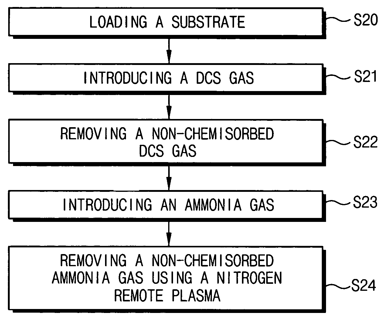
[0199] Silicon nitride (SiN) layers were formed on substrates using processes substantially identical to those described with reference to FIGS. 8 to 11, respectively. In the processes forming the silicon nitride layers according to the Examples 1 to 4, DCS gases and NH3 gases were provided for about 20 seconds and about 35 seconds, respectively.

example 5

[0200] A hafnium oxide (HfO2) layer was formed on a substrate using processes substantially identical to that described with reference to FIG. 12. To form the hafnium oxide layer, TEMAH was used as a first reactant and ozone (O3) was used as a second reactant. Additionally, an argon plasma was used as a purge gas and as a plasma for removing impurities was applied to remove impurities from the hafnium oxide layer. A deposition ratio was about 0.7 Å / cycle, and the hafnium oxide layer had a thickness of about 40 Å.


PUM

PropertyMeasurementUnit
temperatureaaaaaaaaaa

Abstract

In a method of forming a layer using an atomic layer deposition process, after a substrate is loaded into a chamber, a first reactant is provided onto the substrate. The first reactant is partially chemisorbed on the substrate. A second reactant is introduced into the chamber to form a preliminary layer on the substrate by chemically reacting the second reactant with the chemisorbed first reactant. Impurities in the preliminary layer and unreacted reactants are simultaneously removed using a plasma for removing impurities to thereby form the layer on the substrate. The impurities in the layer may be effectively removed so that the layer may have reduced leakage current.

Description

CROSS-REFERENCE TO RELATED APPLICATIONS [0001] This application claims priority under 35 USC § 119 to Korean Patent Application No. 2004-38058 filed on May 28, 2004, the content of which is incorporated herein by reference in its entirety. In addition, this application is a continuation-in-part application of and claims priority under 35 U.S.C. § 120 of co-pending U.S. patent application Ser. No. 10 / 403,572 filed on Mar. 31, 2003 and entitled “METHOD OF FORMING A THIN FILM WITH A LOW HYDROGEN CONTENT”, which claims priority under 35 U.S.C. § 119 from Korean Patent Application No. 2002-31724 filed on Jun. 5, 2002, both of which are incorporated herein by the reference in their entirety.BACKGROUND OF THE INVENTION [0002] 1. Field of the Invention [0003] Exemplary embodiments of the present invention relate to methods of forming a layer and methods of forming a semiconductor capacitor having the layer. More particularly, exemplary embodiments of the present invention relate to methods ...

Claims


Application Information

Patent Timeline
Patent Type & Authority Applications(United States)
IPC IPC(8): H01L21/20H01L21/44
CPCC23C16/0245C23C16/4554C23C16/45546H01L21/3141H01L28/90H01L21/31637H01L21/31645H01L21/3185H01L28/40H01L21/31604H01L21/0228H01L21/0234H01L21/02334
Inventor LEE, JONG-CHEOLIM, KI-VINKIM, SUNG-TAEKIM, YOUNG-SUNYOO, CHA-YOUNGCHOI, HAN-MEINAM, GAB-JINLEE, SEUNG-HWAN
Owner SAMSUNG ELECTRONICS CO LTD
Why Eureka
Try Eureka