Silicon wafer, its manufacturing method, and its manufacturing apparatus

Inactive Publication Date: 2006-01-26
SUMCO TECHXIV
View PDF8 Cites 31 Cited by
  • Summary
  • Abstract
  • Description
  • Claims
  • Application Information

AI Technical Summary

Benefits of technology

[0125] In the pulling step, the silicon single crystal is pulled while the growth condition V/G (V: growth rate, G: axial temperature gradient of the crystal) is adjusted such that void defects, OSFs (oxidation induced stacking faults), and dislocation clusters (interstitial silicon type dislocation defects) are eliminated from the pulled silicon single crystal. At this point, as shown in FIG. 21, the carbon concentration in the silicon single crystal is 3×10¹⁵ atoms/cm3 or less, and the allowable range of the growth condition V/G under which defect-free crystals can be obtained

Problems solved by technology

However, crystal defects called grown-in defects (defects that are introduced in the growth of the crystal) occur in the process of growing a silicon crystal.
As semiconductor circuits have become smaller and more highly integrated in recent years, it is no longer acceptable for grown-in defects to be present near the surface layer of a silicon wafer where devices are produced.
However, extremely precise pulling control is necessary to manufacture such silicon crystals, and another drawback is poor productivity.
One way to obtain a silicon wafer that includes no COPs or other grown-in defects near the surface layer where a device circuit is produced is a method in which “a defect-free layer is grown on the wafer surface by epitaxial growth.” A problem with this method, however, is that because a step of forming a layer by epitaxial growth is introduced, the manufacturing cost is higher than with a polished wafer.
A defect-free layer that includes no COPs or the like can similarly be produced as a wafer surface layer by a method involving annealing in a hydrogen or argon atmosphere, but the introduction of an annealing step again drives the cost higher than with a polished wafer.
More specifically, although COPs of about 0.10 μm or larger as measured by particle counter are considered a problem, and must be reduced, it is known that COPs of smaller size will have little effect.
The occurrence and growth of these void defects are greatly affected by the thermal history to which the silicon crystal is subjected during crystal growth.
Also, the elimination of the vacancy supersaturation slows and new void nuclei are generated, and as a result, the void defect density increases, but the void defects to not become large in size.
Therefore, if G1 has a large distribution differential, if the growth rate V is merely lowered in order to achieve a low V/G1, there is the danger that V/G1 will be relatively low around the periphery of the silicon wafer 100, R-OSFs will occur at the periphery, or the void defect size and void defect density will be non-uniform in the wafer plane, leading to partial increases in defect size and density.
Accordingly, as mentioned above, there is the danger that R-OSFs will occur around the wafer periphery, or that partial increases in defect size and density will occur in the wafer plane.
Because there is a limit to the pulling rate, there is the danger that productivity will suffer.
Nevertheless, this only refers in principle to the maximum allowable range of the pulling rate V. The reason for this is that G is usually not consistent in the radial direction.
This means that no change in the pulling rate V is allowed even

Method used


Image

  • Silicon wafer, its manufacturing method, and its manufacturing apparatus
  • Silicon wafer, its manufacturing method, and its manufacturing apparatus
  • Silicon wafer, its manufacturing method, and its manufacturing apparatus

Examples


first embodiment

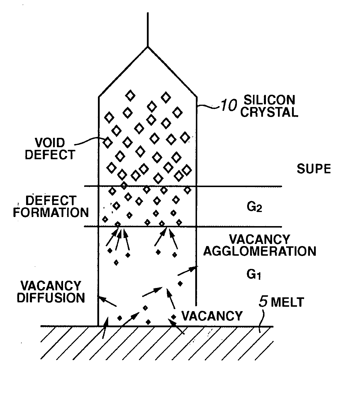
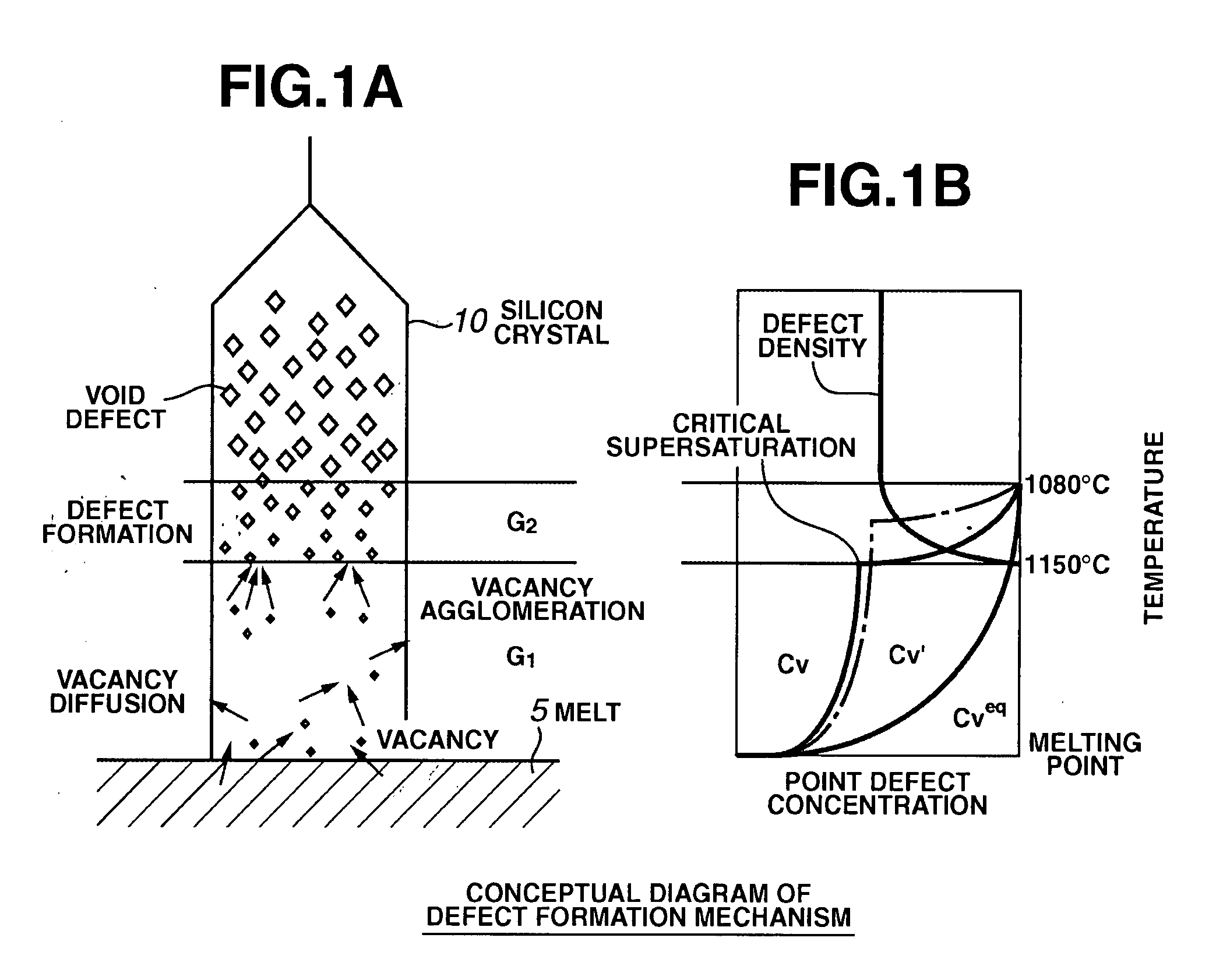
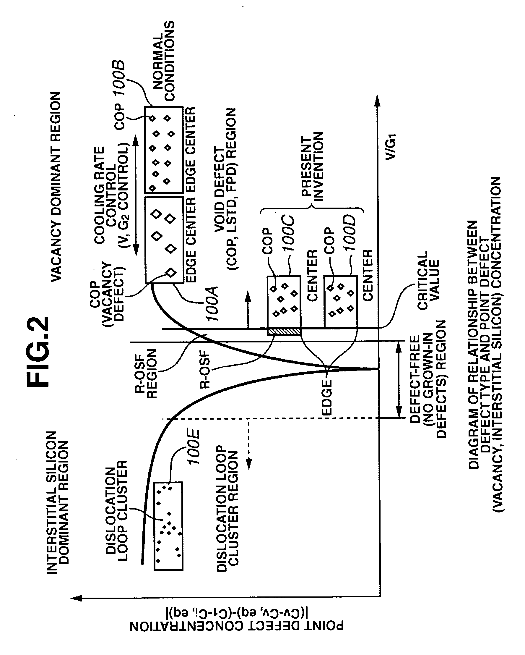
[0185]100D shown in FIG. 2 is a silicon wafer in the first embodiment. The silicon wafer 100D in this embodiment is manufactured such that no OSF region is present anywhere in the plane of the silicon wafer, from the planar center to the edge.

[0186] The region indicated by hatching in FIG. 5 indicates the range of the average void defect density and the average void defect size in the entire plane of the silicon wafer 100D of the first embodiment. The silicon wafer 100D of the present invention has an average void defect density in the entire wafer plane of 5×10⁶ / cm3 or less, and has an average void defect size of 100 nm or less.

[0187] The silicon crystal 10 in the first embodiment has a diameter of 200 mm, and is grown by pulling at a rate V of from 1.11 to 1.45 mm / min.

[0188] With this first embodiment, since the average void defect density in the entire wafer plane is 5×10⁶ / cm3 or less, and the average void defect size is 100 nm or less, deterioration in device characteristics ...

second embodiment

[0267]100C in FIG. 2 is the silicon wafer in the second embodiment. The silicon wafer 100C in this embodiment is manufactured such that no OSFs are present in the plane of the wafer at least from the center of the plane up to 10 mm from the outer periphery.

[0268] The region indicated by hatching in FIG. 5 indicates the range of the average void defect density and the average void defect size in the region to the inside of R-OSF of the silicon wafer 100C of the second embodiment. The silicon wafer 100C in the second embodiment has an average void defect density in the region to the inside of R-OSF of 5×10⁶ / cm3 or less, and has an average void defect size of 100 nm or less.

[0269] The manufacturing method in the second embodiment is as follows.

Manufacturing Method 3

[0270] With this Manufacturing Method 3, the above-mentioned method ⑤ is applied, and the cooler 30 is installed inside the CZ furnace 2. The diameter of the silicon crystal 10 is 200 mm.

[0271] The pulling rate V of th...

third embodiment

[0282] We will now describe an embodiment in which it is possible to expand the allowable range of the growth condition V / G at which a defect-free crystal can be obtained.

[0283]FIG. 25 is a side view of the apparatus constitution in this embodiment.

[0284] As shown in FIG. 25, the single crystal pulling apparatus 101 of this embodiment is equipped with a CZ furnace 102 as a chamber for pulling a single crystal.

[0285] A crucible 103a, in which the raw material polycrystalline silicon is melted and held as a melt 105, is provided inside the CZ furnace 102. The outside of the quartz crucible 103a is covered by a graphite crucible 103b. A main heater 109 for heating and melting the polycrystalline silicon raw material in the quartz crucible 103a is provided to the side on the outside of the quartz crucible 103b.

[0286] An insulating cylinder 113 is provided between the main heater 109 and the inner walls of the CZ furnace 102. A pulling mechanism (not shown) is provided above the quar...


PUM


Abstract

The production yield about defect free devices is improved by so controlling the size and density of void defects that they are under predetermined levels without marring the productivity. The pull-up speed V of a silicon crystal (10) by a pull-up mechanism (4) is controlled, and the rate of cooling by a cooler (30) is also controlled. As a result, the axial temperature gradient G1 at and near the melting point of the silicon crystal (10) is increased. The growth condition V/G1 is lowered to a temperature near the critical value under the condition that the growth rate V lies in the range from 97% to 75% of the limit rate Vmax and that the solid-liquid interface is convex with respect to the melt surface. Thus a silicon crystal (10) is grown by pulling up.

Description

TECHNICAL FIELD [0001] This invention relates to a silicon wafer, its manufacturing method and its manufacturing apparatus, and more particularly relates to a manufacturing method and a manufacturing apparatus with which the size and density of void defects can be reduced, and to a silicon wafer manufactured with these method and apparatus. The present invention also relates to a method for manufacturing a silicon single crystal, and to a silicon single crystal, and more particularly relates to a method for manufacturing a defect-free silicon single crystal in which void defects, OSFs (oxidation induced stacking faults), and dislocation clusters (interstitial silicon dislocation defects) have been eliminated, and to a defect-free silicon single crystal manufactured by this method, and to an apparatus for pulling this defect-free silicon single crystal. BACKGROUND ART [0002] Silicon crystals are manufactured by pulling according to the CZ (Czochralski) method. An ingot of a pulled si...

Claims


Application Information

Patent Timeline
IPC IPC(8): C30B23/00C30B25/00C30B28/12C30B28/14C30B15/00
CPCC30B15/14C30B29/06C30B15/206C30B15/203
Inventor YOKOYAMA, TAKASHIYOSHIHARA, KOJISAISHOJI, TOSHIAKINAKAMURA, KOZOSUEWA, RYOTA
Owner SUMCO TECHXIV
Why Eureka
Try Eureka