Carburized silicon gate insulators for integrated circuits

Inactive Publication Date: 2006-01-26
MICRON TECH INC
View PDF98 Cites 9 Cited by
  • Summary
  • Abstract
  • Description
  • Claims
  • Application Information

AI Technical Summary

Benefits of technology

[0008] The resulting SiC film is preferably amorphous and has low surface state densities. It provides a gate insulator having a much lower tunneling barrier as compared to grown oxides which are widely used today. The lower tunneling barrier results in reduced tunneling times and allows reduction of power supply voltages. Further, charging at interfaces between composite insulators is reduced.

Problems solved by technology

The thicker films require longer time and higher temperature since the formation of SiC is a diffusion limited process.

Method used


Image

  • Carburized silicon gate insulators for integrated circuits
  • Carburized silicon gate insulators for integrated circuits
  • Carburized silicon gate insulators for integrated circuits

Examples


Embodiment Construction

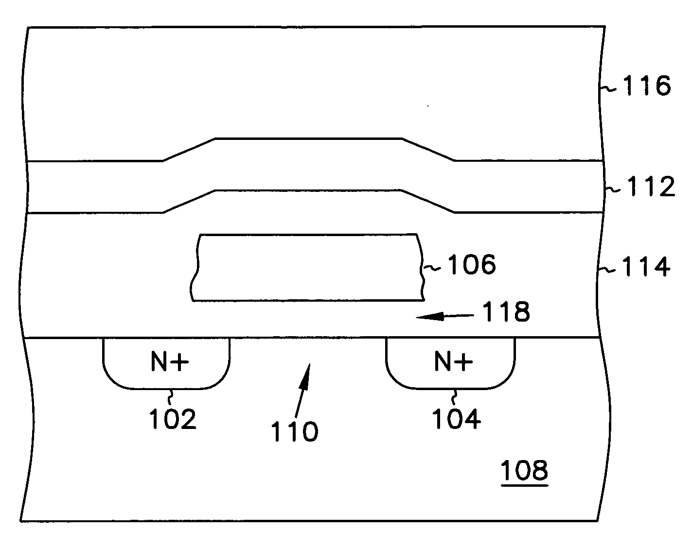
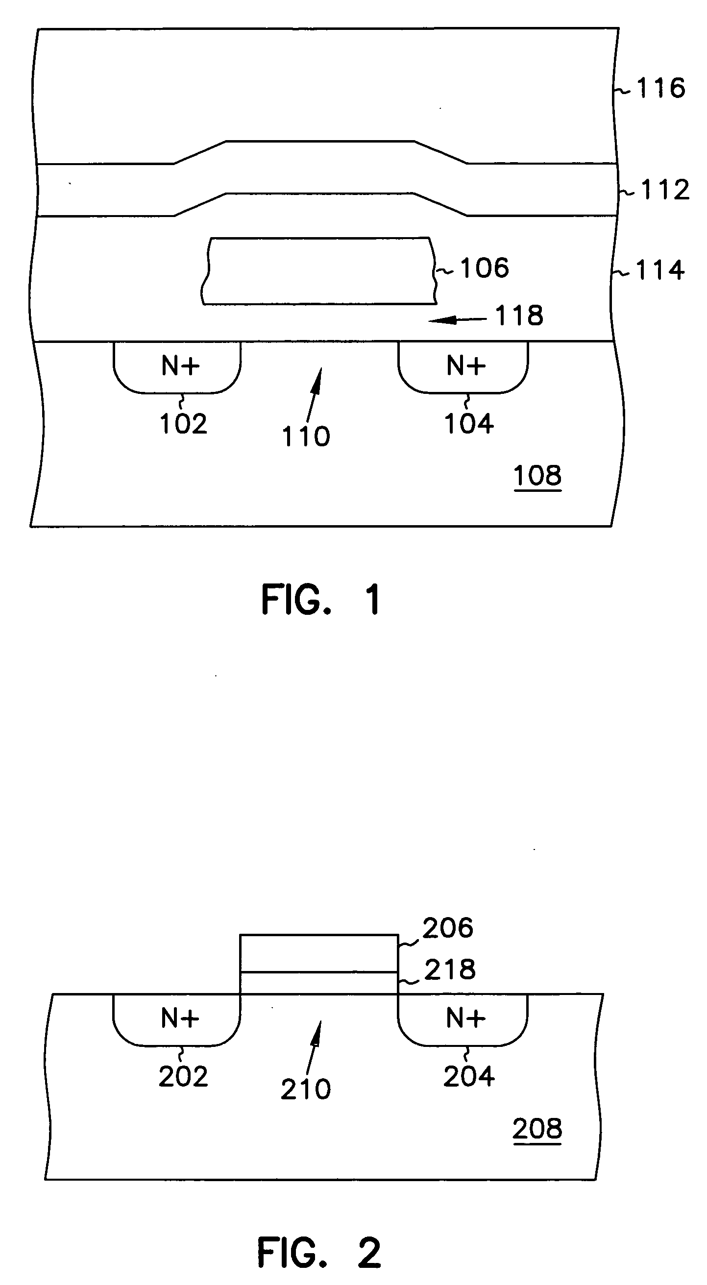
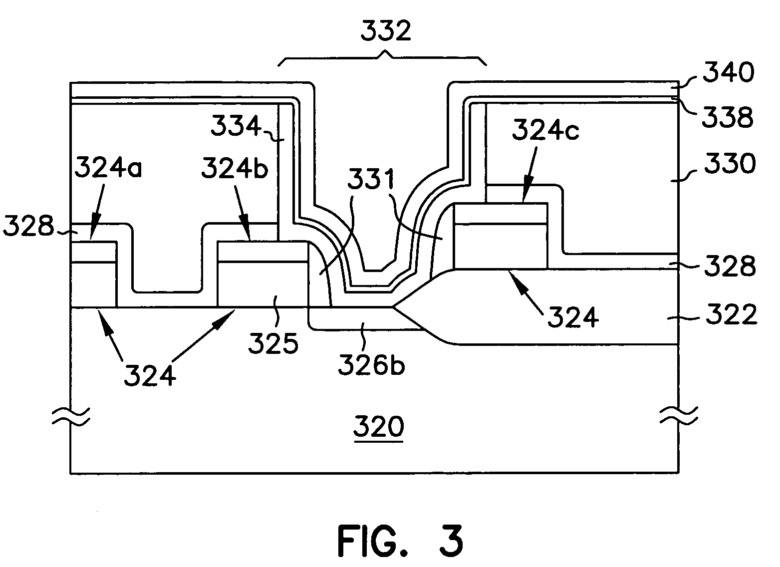
[0016] In the following detailed description, reference is made to the accompanying drawings which form a part hereof, and in which is shown by way of illustration specific embodiments in which the invention may be practiced. These embodiments are described in sufficient detail to enable those skilled in the art to practice the invention, and it is to be understood that other embodiments may be utilized and that structural, logical and electrical changes may be made without departing from the spirit and scope of the present invention. The terms wafer and substrate used in the following description include any semiconductor-based structure having an exposed surface with which to form the integrated circuit structure of the invention. Wafer and substrate are used interchangeably to refer to semiconductor structures during processing, and may include other layers that have been fabricated thereupon. Both wafer and substrate include doped and undoped semiconductors, epitaxial semiconduc...


PUM


Abstract

Silicon carbide films are grown by carburization of silicon to form insulative films. In one embodiment, the film is used to provide a gate insulator for a field effect transistor. The film is grown in a microwave-plasma-enhanced chemical vapor deposition (MPECVD) system. A silicon substrate is first etched in dilute HF solution and rinsed. The substrate is then placed in a reactor chamber of the MPECVD system in hydrogen along with a carbon containing gas. The substrate is then inserted into a microwave generated plasma for a desired time to grow the film. The microwave power varies depending on substrate size. The growth of the film may be continued following formation of an initial film via the above process by using a standard CVD deposition of amorphous SiC. The film may be used to form gate insulators for FET transistors in DRAM devices and flash type memories. It may be formed as dielectric layers in capacitors in the same manner.

Description

CROSS-REFERENCE TO RELATED APPLICATION [0001] The present application is a continuation of U.S. Ser. No. 08 / 903,453, filed on Jul. 29, 1997, which is herein incorporated by reference in its entirety.FIELD OF THE INVENTION [0002] The present invention relates to semiconductor field effect transistors, and in particular to insulators for gates of field effect transistors. BACKGROUND OF THE INVENTION [0003] Field-effect transistors (FETs) are typically produced using a standard complementary metal-oxide-semiconductor (CMOS) integrated circuit fabrication process. As is well known in the art, such a process allows a high degree of integration such that a high circuit density can be obtained with the use of relatively few well-established masking and processing steps. A standard CMOS process is typically used to fabricate FETs that each have a gate electrode that is composed of n-type conductively doped polycrystalline silicon (polysilicon) material or other conductive materials. [0004] ...

Claims


Application Information

Patent Timeline
IPC IPC(8): H01L29/788G11C16/04
CPCG11C16/0466Y10S438/931H01L21/28194H01L21/28273H01L29/51H01L29/42364H01L27/10852H01L28/40H01L29/4234H01L29/42324H01L29/40114H10B12/033
Inventor FORBES, LEONARDAHN, KIE Y.
Owner MICRON TECH INC
Why Eureka
Try Eureka