Semiconductor device and a manufacturing method of the same

a technology of semiconductor devices and manufacturing methods, applied in the direction of solid-state devices, resistors, basic electric elements, etc., can solve the problems of drastic increase in these losses, insufficient effect to reduce conduction loss or recovery loss, etc., and achieve the effect of improving the conversion efficiency of power supply voltag

Active Publication Date: 2006-02-02
RENESAS ELECTRONICS CORP
View PDF12 Cites 66 Cited by
  • Summary
  • Abstract
  • Description
  • Claims
  • Application Information

AI Technical Summary

Benefits of technology

[0023] Since the SBD can be formed satisfactorily in a semiconductor chip having the field effect transistor and metal gate interconnect, an inductance of the interconnect for connecting the field effect transistor and the SBD can be reduced. This leads to an improvement in the conversion efficiency of the power supply voltage of a semiconductor device.

Problems solved by technology

As a result, even the connection of the SBD having a forward voltage lower than that of a body diode does not bring about sufficient effects for reducing the conduction loss or recovery loss of the diode.
The present inventors have however found for the first time that when the gate resistance of the low-side power MOS•FET exceeds a predetermined value as a result of a current increase and frequency heightening as described above, a self turn-on phenomenon becomes rapidly eminent, causing a drastic increase in these losses.

Method used


Image

  • Semiconductor device and a manufacturing method of the same
  • Semiconductor device and a manufacturing method of the same
  • Semiconductor device and a manufacturing method of the same

Examples


embodiment 1

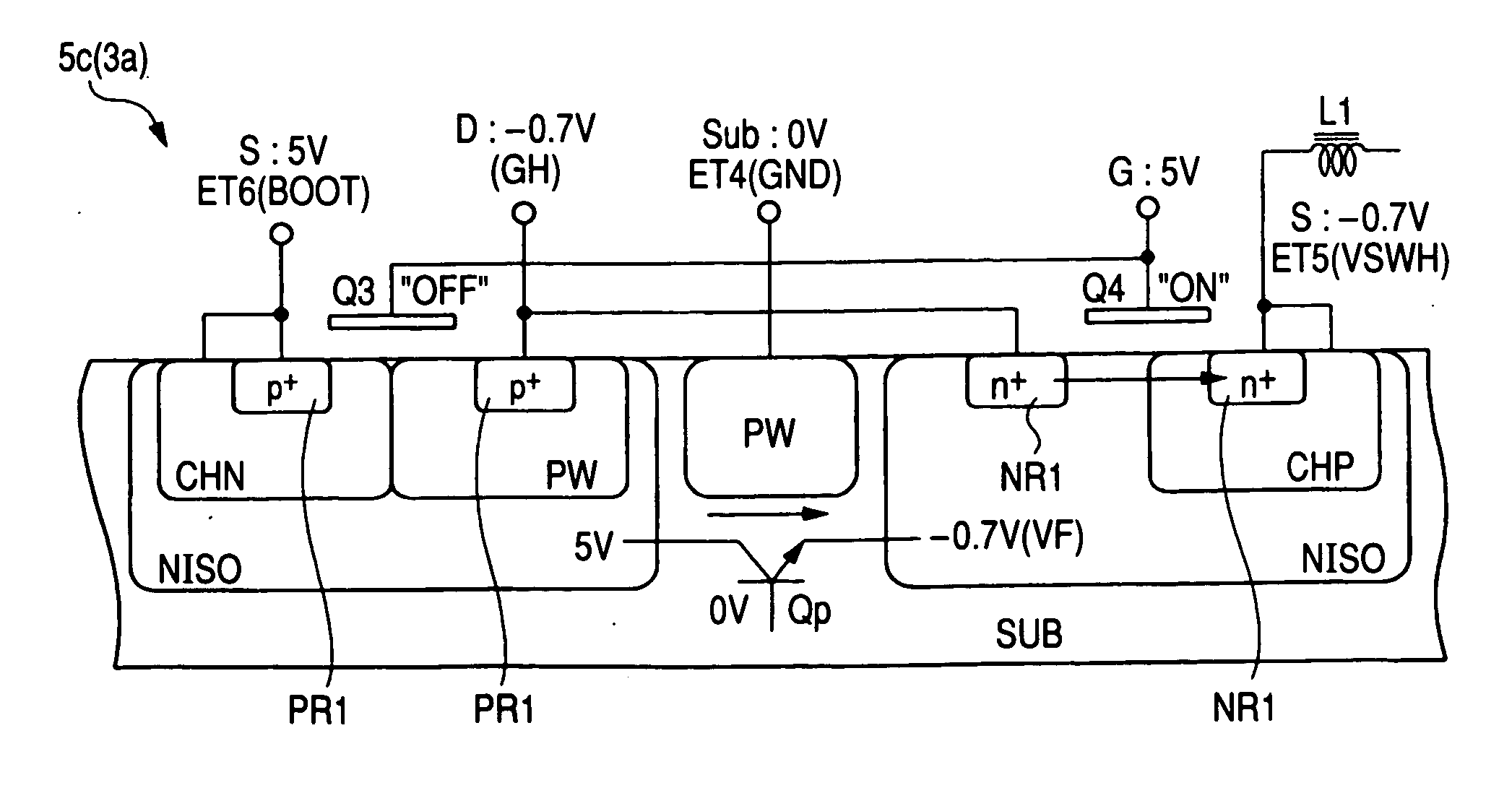
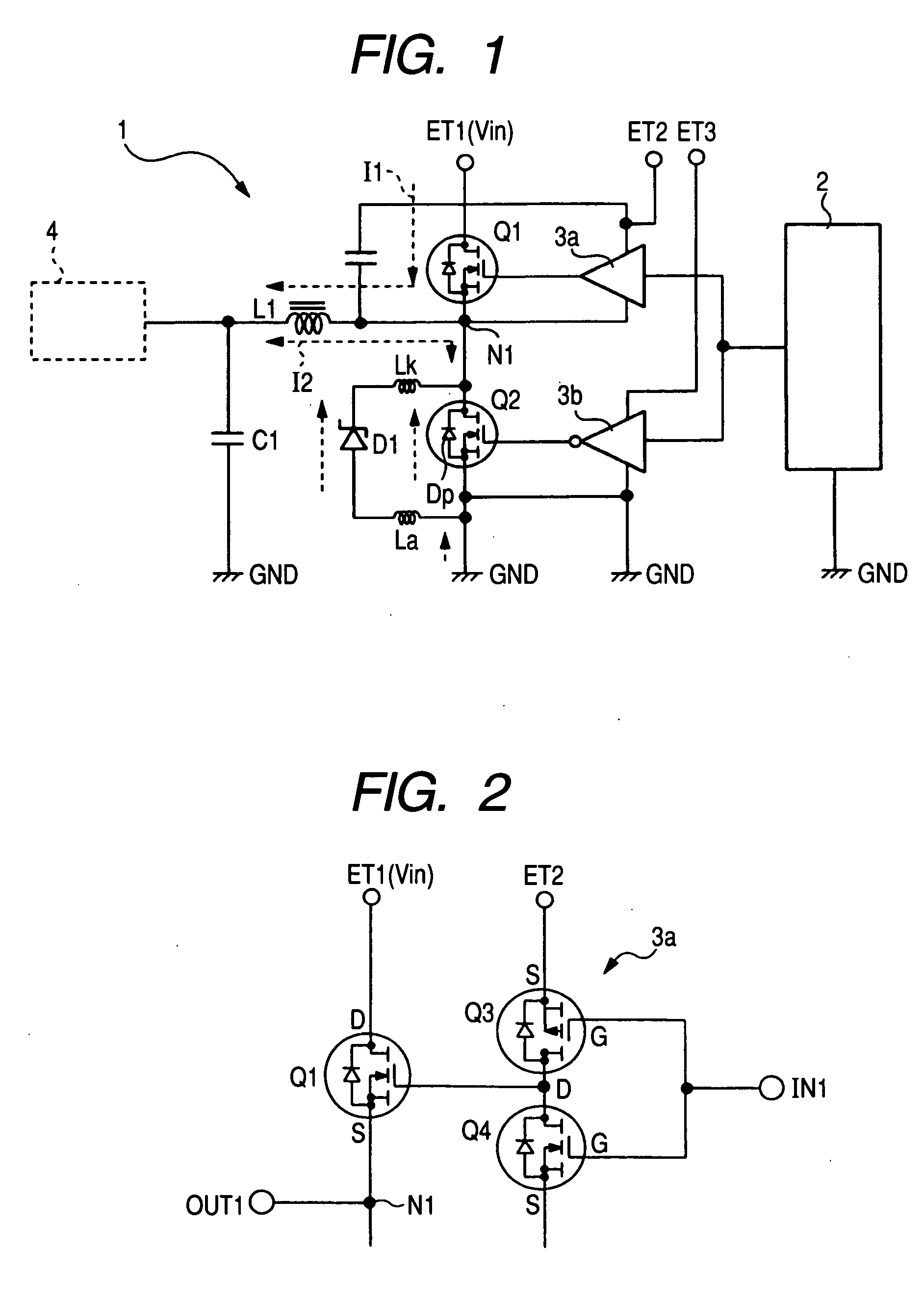
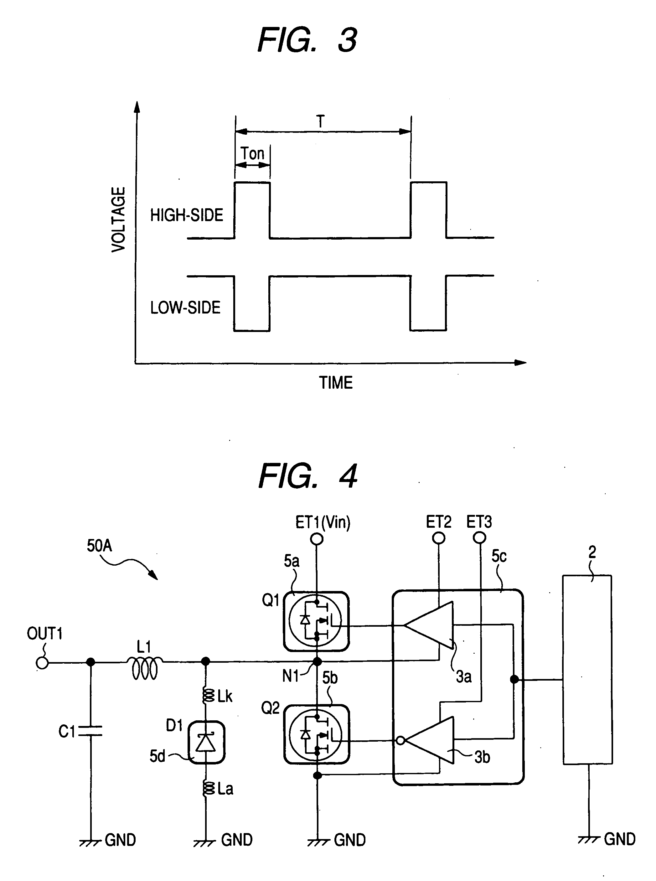
[0092] A semiconductor device according to Embodiment 1 is a non-insulated DC-DC converter to be used in a power supply circuit of electronic devices such as desktop personal computers, laptop personal computers, servers and game machines. FIG. 1 illustrates one example of a circuit diagram of the non-insulated DC-DC converter 1. The non-insulated DC-DC converter 1 has elements such as control circuit 1, driver circuits (first and second control circuits) 3a, 3b, power MOS (first and second field effect transistors) Q1, Q2, SBD (Schottky Barrier Diode) D1, coil L1 and condenser C1.

[0093] The control circuit 2 is a circuit for supplying a signal controlling the width (on time) of a voltage switch-on of the power MOS Q1, Q2 such as pulse width modulation (PWM) circuit. This control circuit 2 is housed in a package different from that of the power MOS Q1, Q2. The outputs (terminals for control signal) of this control circuit 2 are electrically connected to the inputs of the driver cir...

embodiment 2

[0136] A modification example of the disposing position of the SBD in a semiconductor chip will be described in Embodiment 2. FIG. 25 is an overall plan view of a semiconductor chip 5b, while FIG. 26 is an overall plan view of the semiconductor chip 5b after addition of the wire WA and external electrode 7E to the semiconductor chip 5b of FIG. 25. Although FIGS. 25 and 26 are plan views, gate fingers 6a and 6b and pad BP1 are hatched to facilitate the understanding of the diagrams.

[0137] In this Embodiment 2, the formation region SDR of the SBD D1 is disposed near the long side on one side of the semiconductor chip 5b. In particular, the formation region SDR of the SBD D1 is disposed on a long side near the external electrode 7E as illustrated in FIG. 26. By such an arrangement, a parasitic inductance on the anode side of the SBD D1 can be reduced, whereby a larger current can be transferred to the SBD D1. This enables a more reduction in the conduction loss and recovery loss of th...

embodiment 3

[0139] In Embodiment 3, another modification example of the arrangement position of the SBD in a semiconductor chip will be described. FIG. 27 is an overall plan view of a semiconductor chip 5b, while FIG. 28 is an overall plan view of the semiconductor chip 5b after addition of a wire WA and an external electrode 7E to FIG. 27. FIGS. 27 and 28 are each a plan view, but gate fingers 6a, 6b and pad BP1 are hatched to facilitate the understanding of these diagrams.

[0140] In Embodiment 3, the formation region SDR of the SBD D1 is disposed near one short side of the semiconductor chip 5b. The formation region SDR of the SBD D1 extends along the short side (second direction Y) of the semiconductor chip 5b. In particular, as illustrated in FIG. 28, the formation region SDR of the SBD D1 is disposed on a short side near the external electrode 7E. By such an arrangement, a parasitic inductance on the anode side of the SBD D1 can be reduced and therefore, a larger current can be transferred...


PUM


Abstract

In a non-insulated DC-DC converter having a circuit in which a power MOS•FET high-side switch and a power MOS•FET low-side switch are connected in series, the power MOS•FET low-side switch and a Schottky barrier diode to be connected in parallel with the power MOS•FET GF low-side switch are formed within one semiconductor chip. The formation region SDR of the Schottky barrier diode is disposed in the center in the shorter direction of the semiconductor chips and on both sides thereof, the formation regions of the power MOS•FET low-side switch are disposed. From the gate finger in the vicinity of both long sides on the main surface of the semiconductor chip toward the formation region SDR of the Schottky barrier diode, a plurality of gate fingers are disposed so as to interpose the formation region SDR between them.

Description

CROSS-REFERENCE TO RELATED APPLICATION [0001] The present application claims priority from Japanese patent application No. 2004-223664 filed on 30 Jul., 2004, the content of which is hereby incorporated by reference into this application. BACKGROUND OF THE INVENTION [0002] The present invention relates to a semiconductor device and a manufacturing technology thereof, particularly to a technology effective when applied to a semiconductor device having a power supply circuit and a manufacturing method thereof. [0003] A DC-DC converter widely used as one of power supply circuits has a high-side power MOS•FET (Metal Oxide Semiconductor Field Effect Transistor) and a low-side power MOS•FET connected to each other in series. The high-side power MOS•FET has a switching function for controlling a DC-DC converter, while the low-side power MOS•FET has a switching function for synchronous rectification. These two power MOS•FETs perform voltage conversion by being alternately turned ON / OFF whil...

Claims


Application Information

Patent Timeline
Patent Type & Authority Applications(United States)
IPC IPC(8): H01L29/00
CPCH01L23/3107H01L23/49524H01L23/49562H01L23/49575H01L24/06H01L24/40H01L24/45H01L24/49H01L24/73H01L29/1095H01L29/41741H01L29/4232H01L29/4238H01L29/456H01L29/7806H01L29/7813H01L29/872H01L2224/0401H01L2224/05624H01L2224/45015H01L2224/45144H01L2224/48011H01L2224/48091H01L2224/48095H01L2224/48137H01L2224/48247H01L2224/48253H01L2224/4903H01L2224/49051H01L2224/49111H01L2224/49171H01L2224/49175H01L2924/01002H01L2924/01004H01L2924/01005H01L2924/01013H01L2924/01014H01L2924/01015H01L2924/01022H01L2924/01027H01L2924/01028H01L2924/01029H01L2924/01033H01L2924/01046H01L2924/01047H01L2924/0105H01L2924/01057H01L2924/01074H01L2924/01078H01L2924/01079H01L2924/01082H01L2924/014H01L2924/13091H01L2924/14H01L2924/1532H01L2924/19041H01L2924/19043H01L2924/20753H01L2924/20755H01L2924/30105H01L2924/30107H01L2924/3011H02M7/003H01L24/48H01L2924/01006H01L2924/01021H01L2924/01023H01L2924/01072H01L2224/48624H01L2224/73221H01L2224/40247H01L2224/05554H01L2924/1306H01L2924/12032H01L2924/1305H01L2924/00014H01L2924/00H01L2924/181H01L2224/40095H01L2224/40245H01L2224/04042H01L2224/371H01L2224/84801H01L2224/37124H01L2224/37147H01L2224/8385H01L2224/8485H01L24/37H01L2224/32245H01L2224/73265H01L2224/0603H02M3/003H01L24/84H01L2924/00012H01L24/34H01L24/39H01L29/7811H01L21/28035H01L21/823475H01L27/0629H01L29/4236H01L29/45H01L29/4916H01L29/66143H01L29/66734H02M3/155
Inventor SHIRAISHI, MASAKIUNO, TOMOAKIMATSUURA, NOBUYOSHI
Owner RENESAS ELECTRONICS CORP
Why Eureka
Try Eureka