Deposition methods for the formation of polycrystalline materials on mobile substrates

a technology of polysilicon and polycrystalline silicate, which is applied in the direction of chemical vapor deposition coating, solid-state devices, coatings, etc., can solve the problems of poor structural stability, unsuitable for performing logic and mixed signal functions necessary to drive the display, and achieve the effect of enhancing chemical vapor deposition

Inactive Publication Date: 2006-02-02
OVSHINSKY STANFORD R
View PDF8 Cites 47 Cited by
  • Summary
  • Abstract
  • Description
  • Claims
  • Application Information

AI Technical Summary

Problems solved by technology

The most common switching devices are TFT transistors made from amorphous silicon (a-Si) because a-Si can be deposited over large area substrates (e.g. glass plates) at relatively low temperatures (300-400° C.). a-Si, however, is not an optimum switching device material because it has poor structural stability upon exposure to light over time and because it possesses a low charge carrier mobility.
Although adequate for the purposes of switching individual pixels on and off, the low mobility of a-Si renders it unsuitable for performing the logic and mixed signal functions necessary to drive the display.
The need for external driver circuits further complicates the fabrication of liquid crystal displays, increases the overall device footprint, and increases power consumption.
Since switching devices block the transmission of backlighting through a display, smaller switching devices lead to higher light throughput and higher display aperture ratios.
In spite of the advantageous material properties of polysilicon, its use in active matrix liquid crystal displays (and active matrix organic light emitting diode displays, a display technology that would also benefit from polysilicon switching devices) has been limited because polysilicon is a more difficult material to deposit than a-Si.

Method used


Image

  • Deposition methods for the formation of polycrystalline materials on mobile substrates
  • Deposition methods for the formation of polycrystalline materials on mobile substrates

Examples


Embodiment Construction

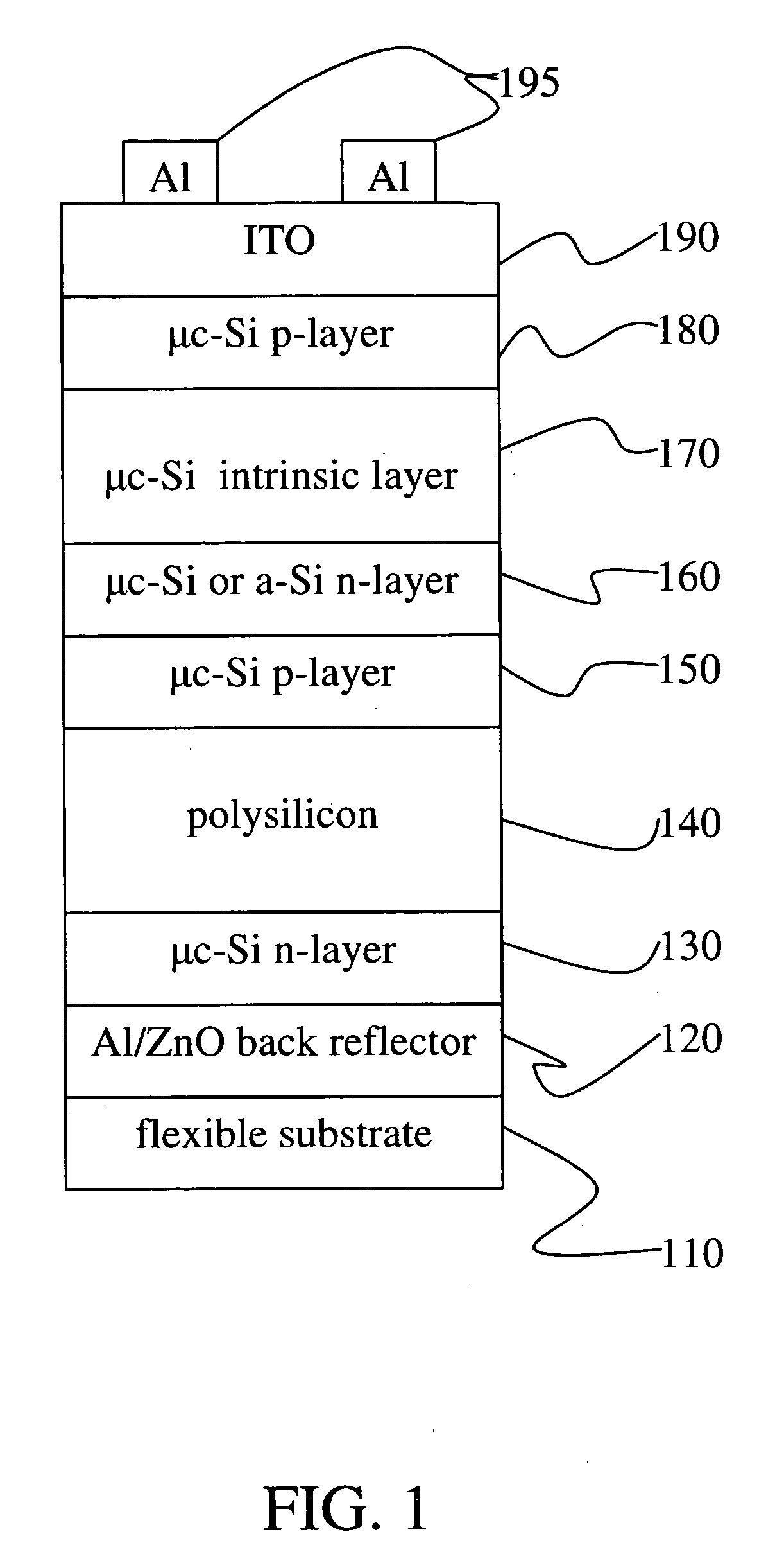
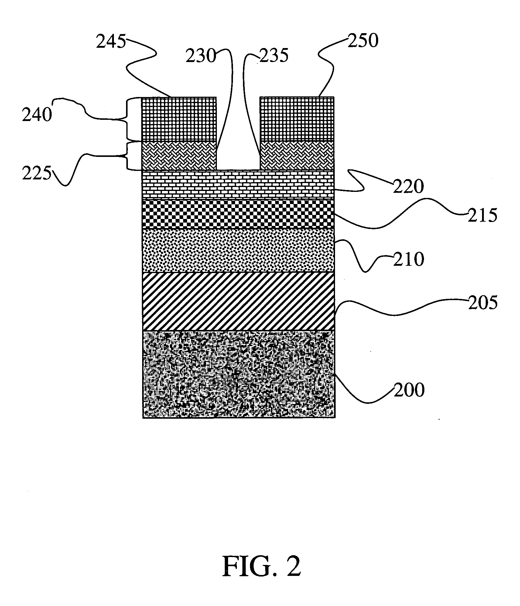
[0019] The instant invention provides a process and apparatus for the deposition of a polycrystalline material in a continuous manufacturing process. The instant invention addresses the need for high volume deposition of polycrystalline materials and devices including same for display and other applications. In a preferred embodiment, the polycrystalline material is polysilicon or polycrystalline SiGe. The instant deposition apparatus includes one or more deposition chambers for depositing one or more layers on a continuously mobile substrate where at least one of the deposited layers is polysilicon or polycrystalline SiGe or where at least one of the deposited layers is amorphous or microcrystalline silicon or SiGe and where the amorphous or microcrystalline silicon or SiGe is transformed into polysilicon or polycrystalline SiGe in a deposition chamber or processing chamber of the apparatus. Single layer polysilicon depositions or multilayer structures that include a polysilicon an...


PUM

PropertyMeasurementUnit
grain sizeaaaaaaaaaa

Abstract

A deposition apparatus and method for continuously depositing a polycrystalline material such as polysilicon or polycrystalline SiGe layer on a mobile discrete or continuous web substrate. The apparatus includes a pay-out unit for dispensing a discrete or continuous web substrate and a deposition unit that receives the discrete or continuous web substrate and deposits a series of one or more thin film layers thereon in a series of one or more deposition or processing chambers. In a preferred embodiment, polysilicon is formed by first depositing a layer of amorphous or microcrystalline silicon using PECVD and transforming said layer to polysilicon through heating or annealing with one or more lasers, lamps, furnaces or other heat sources. Laser annealing utilizing a pulsed excimer is a preferred embodiment. By controlling the processing temperature, temperature distribution within a layer of amorphous or microcrystalline silicon etc., the instant deposition apparatus affords control over the grain size of polysilicon. Passivation of polysilicon occur through treatment with a hydrogen plasma. Layers of polycrystalline SiGe may similarly be formed. The instant deposition apparatus provides for the continuous deposition of electronic devices and structures that include a layer of a polycrystalline material such as polysilicon and / or polycrystalline SiGe. Representative devices include photovoltaic devices and thin film transistors. The instant deposition apparatus also provides for the continuous deposition of chalcogenide switching or memory materials alone or in combination with other metal, insulating, and / or semiconducting layers.

Description

CROSS-REFERENCE TO RELATED APPLICATIONS [0001] This application is a continuation of U.S. application Ser. No. 10 / 440,664 entitled “Deposition Apparatus for the Formation of Polycrystalline Materials on Mobile Substrates”, filed May 19, 2003; the disclosure of which is hereby incorporated by reference herein.FIELD OF INVENTION [0002] This invention relates to the continuous deposition of a polycrystalline material. More particularly, this invention pertains to an apparatus for depositing polysilicon and polycrystalline SiGe on mobile discrete or continuous web substrates. Most particularly, this invention relates to the continuous deposition of amorphous or microcrystalline silicon or SiGe and its transformation to polysilicon or polycrystalline SiGe in a continuous process. BACKGROUND OF THE INVENTION [0003] Consumer and industrial interest in display technologies continues to grow as displays become more powerful and compact. New applications for displays continue to be developed ...

Claims


Application Information

Patent Timeline
Patent Type & Authority Applications(United States)
IPC IPC(8): C23C16/00C23C16/54
CPCC23C16/24H01L29/78603H01L27/1214C23C16/545
Inventor OVSHINSKY, STANFORD R.
Owner OVSHINSKY STANFORD R
Why Eureka
Try Eureka