Copper damascene barrier and capping layer

a technology of imd layer and barrier layer, which is applied in the direction of semiconductor/solid-state device manufacturing, basic electric elements, electric apparatus, etc., can solve the problems of difficult metal interconnection technology, reduced electrical interconnection effectiveness and electrical insulation properties of imd layer, and easy diffusion of copper into imd layer, etc., to achieve the effect of improving electrical properties

Inactive Publication Date: 2006-02-02
WU ZHEN CHENG +3
View PDF12 Cites 211 Cited by
  • Summary
  • Abstract
  • Description
  • Claims
  • Application Information

AI Technical Summary

Benefits of technology

[0009] To achieve the foregoing and other objects, and in accordance with the purposes of the present invention, as embodied and broadly descri

Problems solved by technology

As device sizes decrease it has been increasingly difficult to provide metal interconnection technology that satisfies the requirements of low RC (resistance capacitance), particularly where device sizes decrease to about 0.1 microns and smaller.
The use of copper for device interconnects has created a number of constantly changing technological problems in semiconductor device manufacturing that must be overcome to provide reliable devices.
One problem with copper interconnects has been the fact that copper readily diffuses through silicon dioxide or silicon oxide based materials, a typical IMD material.
The diffusion of copper into the IMD layer reduces both the effectiveness of the electrical interconnect and the electrical insulation properties of the IMD layers.
Another problem is that copper has poor adhesion to silicon oxide based IMD layer

Method used


Image

  • Copper damascene barrier and capping layer
  • Copper damascene barrier and capping layer
  • Copper damascene barrier and capping layer

Examples


Embodiment Construction

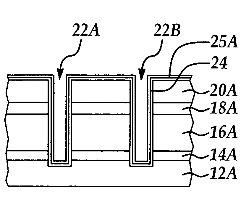
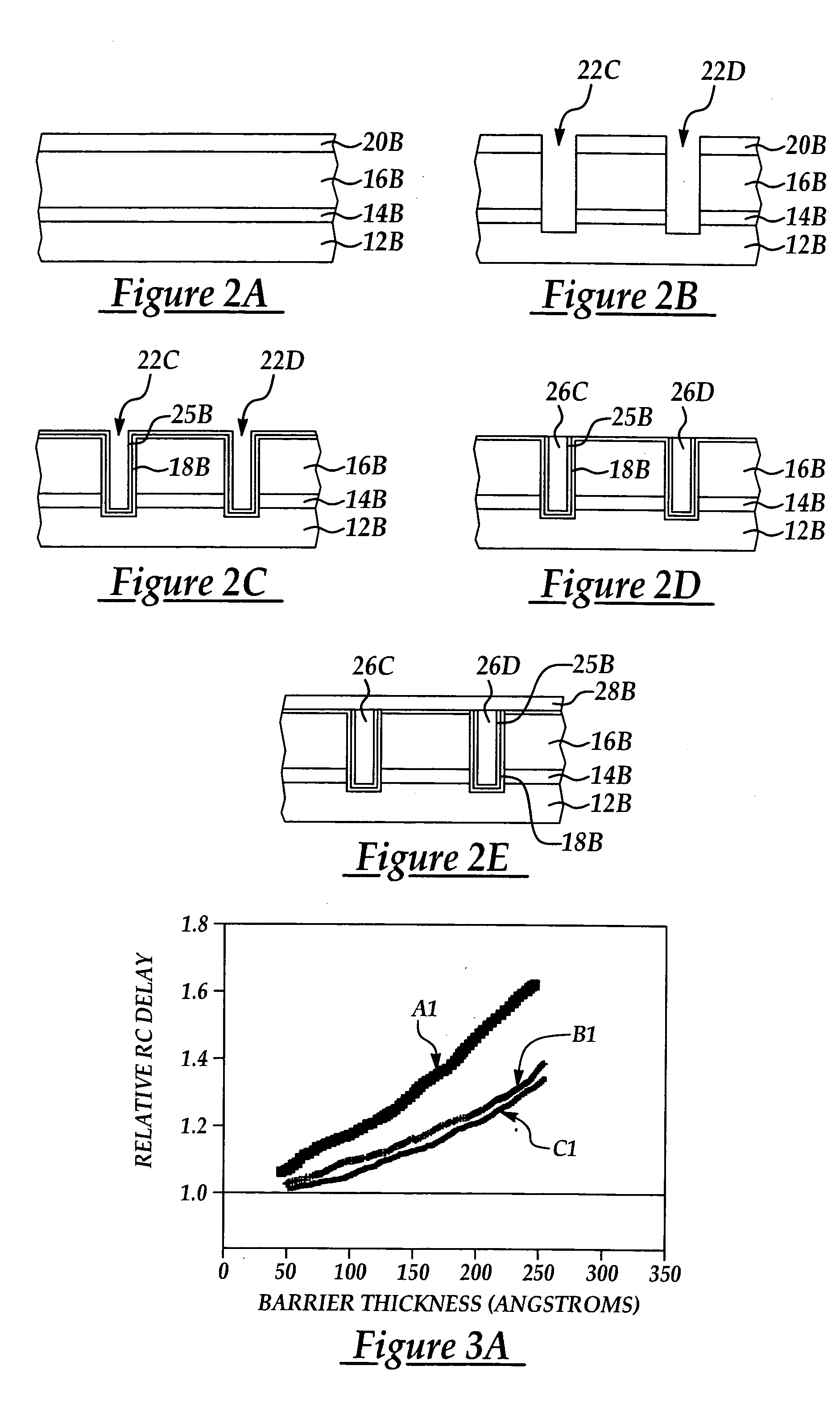
[0015] Although the method of the present invention is explained by exemplary reference the formation of copper damascene structures in a multi-level semiconductor device it will be appreciated that the method of the present invention is equally applicable to the formation of dual or single damascene structures including use of other filling metals such as copper alloys, tantalum, aluminum, and alloys thereof. The method of the present invention is advantageously used to form metal damascenes, particularly copper damascenes, to improve electrical performance including reducing capacitance contributions to RC signal propagation delay, reducing current leakage, reducing the incidence of time dependent dielectric breakdown (TDDB) by improving time to dielectric breakdown, avoiding CMP of a dielectric insulating layer including a low-K dielectric insulating layer to avoid scratching defects, and increasing a resistance to stress induced crack propagation through a dielectric insulating ...


PUM


Abstract

A method for forming a damascene with improved electrical properties and resulting structure thereof including providing at least one dielectric insulating layer overlying a first etch stop layer; forming an anti-reflectance coating (ARC) layer prior to a photolithographic patterning process; forming at least one opening extending through a thickness portion of the at least one dielectric insulating layer and first etch stop layer according to said photolithographic patterning and an etching process; blanket depositing a barrier layer including material selected from the group consisting of silicon carbide and silicon oxycarbide to line the at least one opening; blanket depositing a refractory metal liner over the barrier layer; blanket depositing at least one metal layer to fill the at least one opening; and, removing at least the at least one metal layer overlying the at least one opening level according to a chemical mechanical polish (CMP) process.

Description

FIELD OF THE INVENTION [0001] This invention generally relates to multi-layered semiconductor structures and more particularly to an improved copper damascene and method for forming the same with barrier layers and capping layers provided for improved electrical performance. BACKGROUND OF THE INVENTION [0002] The escalating requirements for high density and performance associated with ultra large scale integration semiconductor wiring require increasingly sophisticated interconnection technology. As device sizes decrease it has been increasingly difficult to provide metal interconnection technology that satisfies the requirements of low RC (resistance capacitance), particularly where device sizes decrease to about 0.1 microns and smaller. [0003] In the fabrication of semiconductor devices, increased device density and interconnect requirements has made the provision of multiple metallization levels extending through multiple dielectric insulating levels necessary. Signal transport s...

Claims


Application Information

Patent Timeline
IPC IPC(8): H01L21/4763
CPCH01L21/76829H01L21/76846H01L21/7684H01L21/76831
Inventor WU, ZHEN-CHENGLI, LAIN-JONGLU, YUNG-CHENJANG, SYUN-MING
Owner WU ZHEN CHENG
Why Eureka
Try Eureka