Method of manufacturing semiconductor device

a manufacturing method and semiconductor technology, applied in semiconductor/solid-state device manufacturing, basic electric elements, electric devices, etc., can solve the problems of not being able to apply in the field of liquid crystal display, limiting the transistor size, and not being able to meet the requirements of semiconductor size control

Inactive Publication Date: 2006-02-02
ADVANCED LCD TECH DEVMENT CENT
View PDF3 Cites 29 Cited by
  • Summary
  • Abstract
  • Description
  • Claims
  • Application Information

AI Technical Summary

Problems solved by technology

On the other hand, the method (2) is not employed in today's silicon ULSI technology.
), and therefore, it cannot be applied in the field of liquid crystal display, in which the substrate is formed of a low melting point material such as glass or plastics.
Since the crystal grain size is about 1 to 2 μm at maximum, there occurs limitation that the transistor size must be controlled smaller.
Hence, a very long processing time is required for crystallization.
However, when multiple transistors are formed, however, grain boundaries are formed in the channel regions, so that the mobility is lowed, and the performances (threshold voltage, sub-shred coefficient, mobility) fluctuate among transistors, though the crystallinity within the crystal grains can be made monocrystalline as in the case of the excimer laser crystallization method.
However, since, in the SLS method, nearly half of the laser beam is shielded by the metal mask, the laser energy cannot be utilized effectively.
As a result, it takes a longer time in processing for crystallization.
Hence, the plane orientation of the crystal grains is not uniform, which also leads to fluctuation of performance among transistors.

Method used


Image

  • Method of manufacturing semiconductor device
  • Method of manufacturing semiconductor device
  • Method of manufacturing semiconductor device

Examples


second embodiment

[0073] the method of manufacturing a semiconductor device having quadrangular crystallized region array uniformly arranged in plane orientation on an insulating material substrate will be explained by referring to FIGS. 6D to 6F and 8A to 8D, particularly referring to FIGS. 8A to 8D.

[0074] First, an insulating material substrate 91 (for example, quartz glass, soda glass, borosilicate glass, lead glass, fluoride glass, sapphire, plastic, polyimide, etc.), having a side 74, a notch 75 or a marking 76 (may be on front surface or rear surface of the substrate) as shown in FIGS. 6D to 6F, is prepared (FIG. 8A). An insulating layer 92 (for example, film thickness 500 nm) is formed on this insulating material substrate 91. The insulating layer 92 is, for example, a SiO2 film formed by CVD (for example, plasma CVD or low pressure CVD method) or sputtering method. Alternatively, the insulating layer 92 may be a laminated structure of different materials, for example, SiN and SiO2. Further, i...

first embodiment

[0075] Then, as shown in FIG. 8A, on the entire surface of the semiconductor thin film 93, a protective film 94 (for example, SiO2, SiON, SiN, SOG, or their laminated film) is formed to a thickness of about 300 nm. The protective film 94 prevents contamination from the outside, prevents contamination by particles, and also acts to grow larger crystals since the semiconductor thin film is cooled slowly after the heating step by the laser or xenon flash lamps because of the heat accumulation effect brought about by the heat-insulating property of the protective layer When the insulating layer 92 and semiconductor thin film 93 are patterned, the protective film may be formed on the entire surface of the substrate. The subsequent process is substantially the same as in the first embodiment, and is described only briefly below.

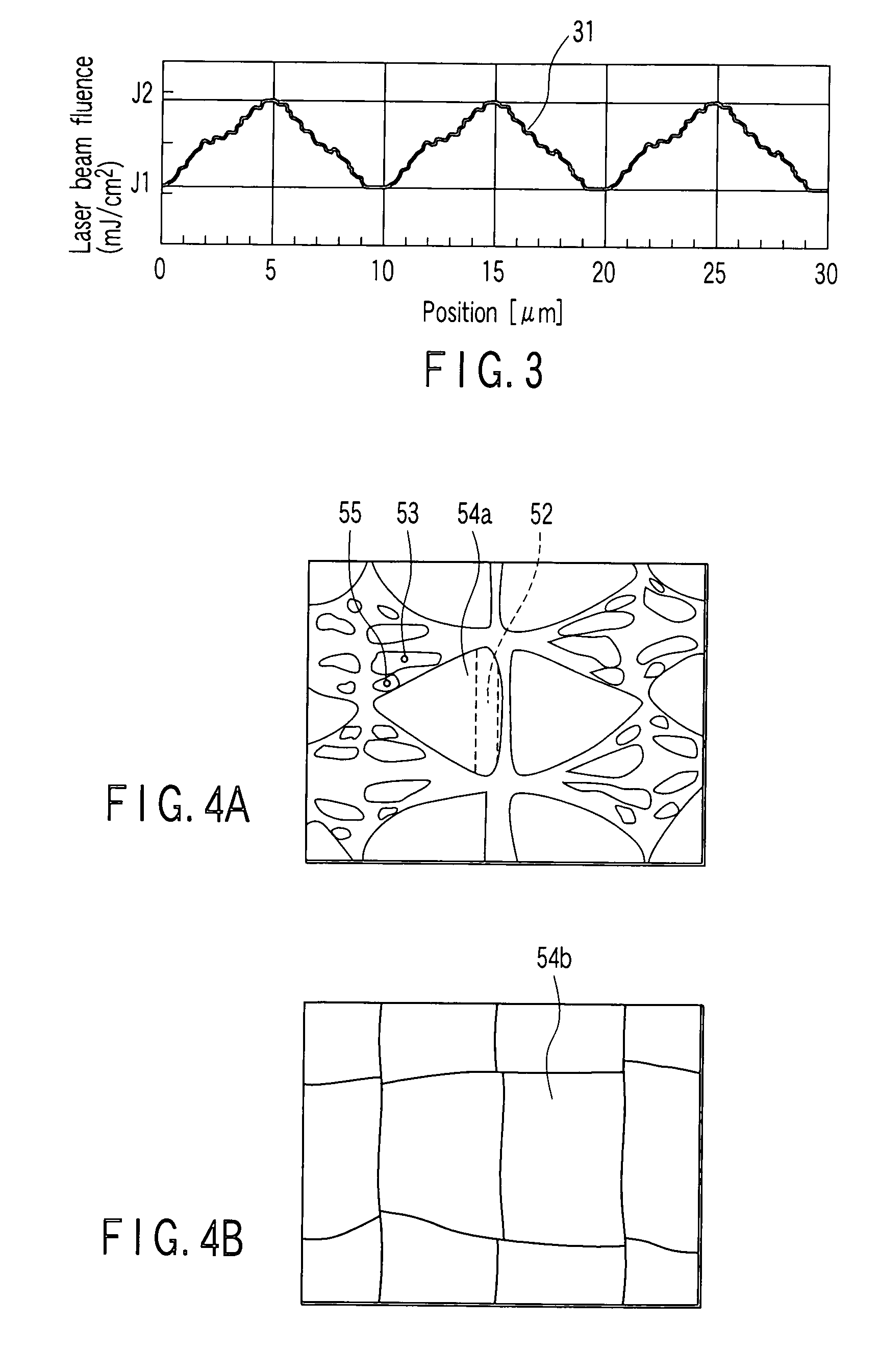
[0076] As shown in FIG. 8B, the surface of the protective film 94 is irradiated with laser beam 85 having light intensity distribution as mentioned above. The main...


PUM


Abstract

A method of manufacturing a semiconductor device includes irradiating a region to be crystallized of a non-monocrystalline semiconductor film with laser beam modulated by an optical modulator to have light intensity distribution having a minimum light intensity line or minimum light intensity spot to crystallize the region, and heating the crystallized region by irradiating light from a flash lamp onto the crystallized region.

Description

CROSS-REFERENCE TO RELATED APPLICATIONS [0001] This application is based upon and claims the benefit of priority from prior Japanese Patent Application No. 2004-220448, filed Jul. 28, 2004, the entire contents of which are incorporated herein by reference. BACKGROUND OF THE INVENTION [0002] 1. Field of the Invention [0003] The present invention relates to a method of manufacturing a semiconductor device, and more particularly to a method of manufacturing a semiconductor device, including crystallizing at least part of a non-monocrystalline semiconductor thin film. [0004] Generally, even a single crystal involves disturbance of atomic rows (such as dislocation), and it is difficult to distinguish “single crystal” from “crystal close to single crystal,” and thus, it should be noted in this specification that “crystal close to single crystal” is also described as “single crystal.”[0005] 2. Description of the Related Art [0006] The SOI (silicon on insulator) technology for forming a mon...

Claims


Application Information

Patent Timeline
Patent Type & Authority Applications(United States)
IPC IPC(8): H01L21/324
CPCH01L21/0237H01L21/0242H01L21/02488H01L21/02529H01L21/324H01L21/02667H01L21/0268H01L21/02686H01L21/268H01L21/02532H01L21/428
Inventor NAKAMURA, HIROKIWARABISAKO, TERUNORIMATSUMURA, MASAKIYO
Owner ADVANCED LCD TECH DEVMENT CENT
Why Eureka
Try Eureka