LSI package equipped with interface module, interface module and connection holding mechanism

Inactive Publication Date: 2006-02-23
KK TOSHIBA
View PDF9 Cites 38 Cited by
  • Summary
  • Abstract
  • Description
  • Claims
  • Application Information

AI Technical Summary

Benefits of technology

[0012] An object of the present invention is to provide an LSI package, which permits eliminating the increase in the manufacturing cost caused by the complex construction of the assembly and permits eliminating the problem in the mounting stage such as the interference of

Problems solved by technology

However, the pace of improvement in the throughput of the interface between LSIs is moderate, compared with the elevation of the clock frequency, so as to generate a bottleneck in the performance of the personal computer.
However, if the number of terminals is increased, the areas of the LSI and the package are increased, giving rise to the limitation that the length of the internal wiring is increased so as to make it impossible to operate at high frequencies.
On the other hand, if the signal frequency per terminal is increased, the attenuation of the electric signal is made large so as to increase the influence given by impedance mismatch to the reflection, with the result that a limitation is generated in the line length.
If a transmission line is to be formed accurately on a mounting board, the manufacturing cost is increased.
In addition, the conductor loss caused by the dielectric loss and the skin effect is increased in accordance with increase in the transmission speed so as to make it difficult to transmit a signal over a sufficiently long distance.
In this assembly, however, it is said to be difficult to maintain the optical accuracy because of the difference in the thermal expansion coefficients of the mounting board and the interposer.
Also, if the optical element is mounted as a bare chip, it is difficult to secure the reliability of the apparatus.
It follows that

Method used


Image

  • LSI package equipped with interface module, interface module and connection holding mechanism
  • LSI package equipped with interface module, interface module and connection holding mechanism
  • LSI package equipped with interface module, interface module and connection holding mechanism

Examples


Example

[0031] (First Embodiment)

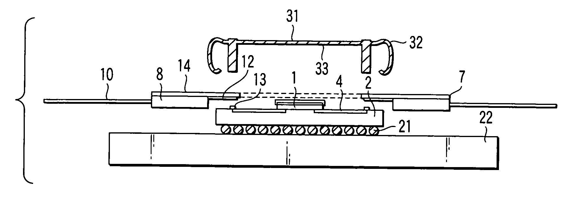
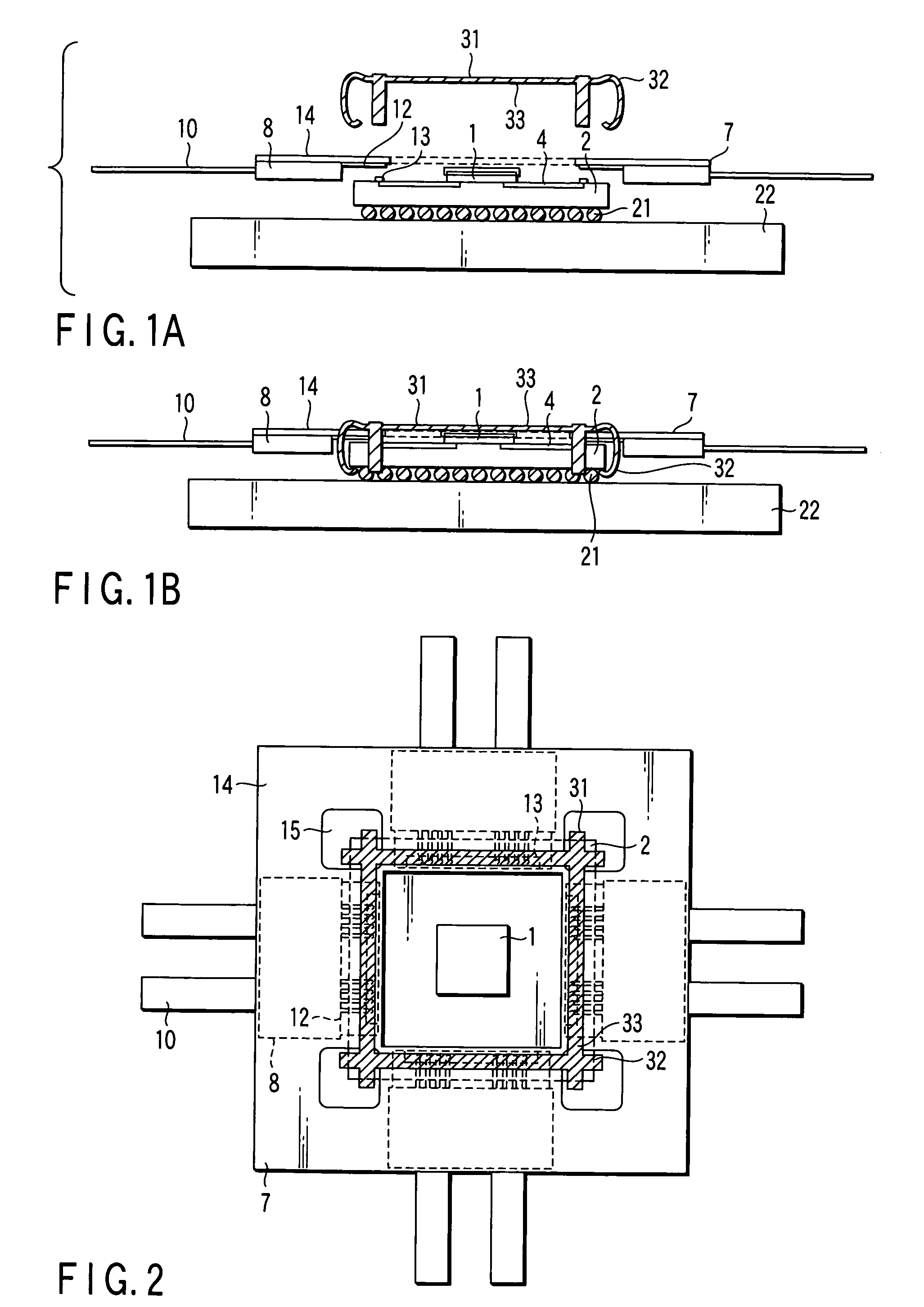
[0032]FIG. 1A is a cross-sectional view schematically showing the construction of an LSI package according to a first embodiment of the present invention before an optical interface module is electrically connected and fixed to the LSI package. On the other hand, FIG. 1B is a cross-sectional view schematically showing the construction of an LSI package comprising the interface module shown in FIG. 1A after the optical interface module is fixed to the LSI package. Further, FIG. 2 is an upper view (plan view) showing the construction of the LSI package comprising the interface module shown in FIG. 1B.

[0033] Incidentally, the LSI package assembly comprising the interface module shown in FIG. 2 is disclosed in U.S. patent application Ser. No. 10 / 778,030, filed by the present inventors (Hamasaki et al) on Feb. 3, 2004. In the following description, the LSI package comprising the interface module shown in FIGS. 1A and 1B is explained briefly on the assumption th...

Example

[0047] (Second Embodiment)

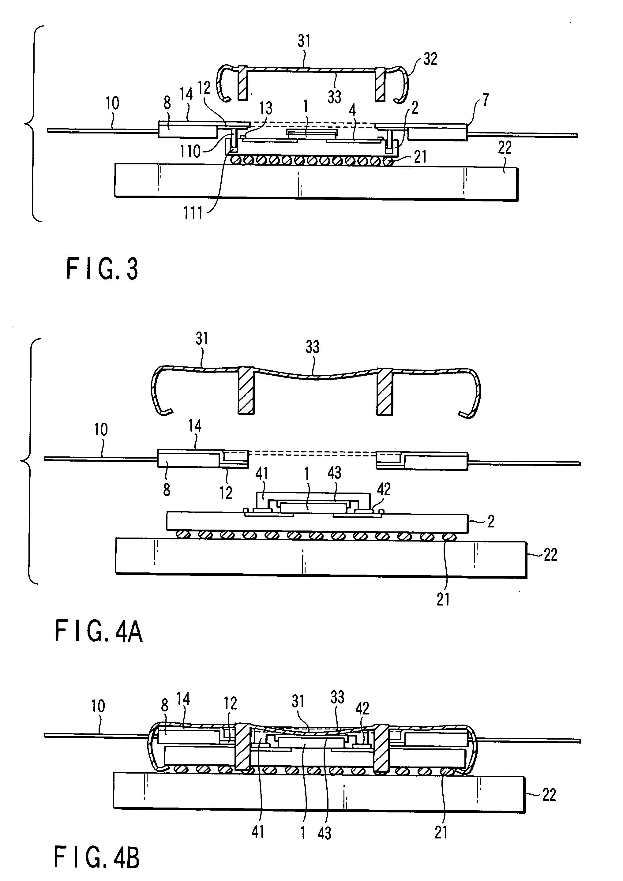
[0048]FIGS. 4A, 4B and 5 collectively show schematically the construction of an LSI package according to a second embodiment of the present invention, wherein FIG. 4A is a cross-sectional view showing the state before the electrical connection and fixation of the optical interface module, FIG. 4B is a cross-sectional view showing the state after the fixation of the optical interface module, and FIG. 5 is a plan view showing the arrangement of the assembly as viewed from above after the connection and fixation. Incidentally, in FIGS. 4A, 4B and 5, the portions equal to those shown in FIG. 1 are denoted by the same reference numerals so as to avoid the overlapping description.

[0049] In the first embodiment, the LSI 1 is mounted in the form of a bare chip on the interposer 2. In the second embodiment, however, the LSI 1 is mounted on the interposer 2 by bonding a heat spreader 41 to the interposer 2 by using an adhesive 42 in order to protect the bare chip a...

Example

[0052] (Third Embodiment)

[0053]FIGS. 6A, 6B, 6C, 7A and 7B collectively show schematically the construction of an LSI package according to a third embodiment of the present invention, wherein FIG. 6A is a cross-sectional view showing the state before the electrical connection and fixation of the optical interface module, FIG. 6B is a cross-sectional view showing the state after the fixation of the optical interface module, FIG. 6C is a cross-sectional view showing the state that a heat sink is mounted on the upper portion. Further, FIG. 7A is a plan view showing the arrangement of the assembly as viewed from above before the clip fixation, and FIG. 7B is a plan view showing the arrangement of the assembly as viewed from above after the clip fixation. Incidentally, in FIGS. 6A, 6B, 6C, 7A and 7B, the portions equal to those shown in FIG. 1 are denoted by the same reference numerals so as to avoid the overlapping description.

[0054] According to the third embodiment of the present in...


PUM


Abstract

I an LSI package, an interface module includes with an interposer having a signal processing LSI mounted thereon and has electric connection terminals for connection to a mounting board and a transmission line for transmitting a high-speed signal to an external wiring. An electric connection terminal is formed in each of the interposer and the interface module for electrically connecting the interposer and the interface module to each other by the mechanical contact, and a fixing holder is mounted for allowing the electric connection terminals to hold the electric connection between the interposer and the interface module. Thus, it is possible to suppress the increase in the manufacturing cost that is caused by the complex construction of the assembly.

Description

CROSS-REFERENCE TO RELATED APPLICATIONS [0001] This application is based upon and claims the benefit of priority from prior Japanese Patent Application No. 2004-237457, filed Aug. 17, 2004, the entire contents of which are incorporated herein by reference. BACKGROUND OF THE INVENTION [0002] 1. Field of the Invention [0003] The present invention relates to an LSI package equipped with an interface module, an interface module and a connection holder, particularly, to an LSI package equipped with an interface module for signal transmission to external wiring of a high-speed signal, an interface module used in the particular LSI package, and a connection holder for holding the connected state between the interface module and an interposer. [0004] 2. Description of the Related Art [0005] In recent years, the clock frequency of an LSI has became higher and higher. In the CPU for a personal computer, a clock frequency which is not lower than GHz order is being put into the practical use. H...

Claims


Application Information

Patent Timeline
IPC IPC(8): H01L23/34
CPCG02B6/3817G02B6/389G02B6/423G02B6/4246H01L2924/0002G02B6/4292H01L2924/00H01L2224/0554H01L2224/05548H01L2224/05573H01L2224/16225H01L2924/00014H01L2224/05599H01L2224/0555H01L2224/0556
Inventor HAMASAKI, HIROSHIFURUYAMA, HIDETO
Owner KK TOSHIBA
Why Eureka
Try Eureka