

Method and apparatus for inspecting semiconductor device
a semiconductor device and method technology, applied in the field of semiconductor device inspection, can solve the problems of deterioration of accuracy, inability to perform size measurement, and inability to so as to improve manufacturing yield, recover or “cure” damage, and quickly grasp the feature quantity
- Summary
- Abstract
- Description
- Claims
- Application Information
AI Technical Summary
Benefits of technology
Problems solved by technology
Method used
Image

Examples
embodiment 1
[0054] In this embodiment, there will be explained one example of a method for inspecting a pattern having its shape with a notch formed in a gate electrode or the like. Note here that the notch of the gate electrode refers to a certain portion in which the width of a lower bottom part of the gate electrode is smaller than an upper bottom thereof. The gate electrode with such the notch defined therein is used from time to time in high-speed devices in order to make the gate length smaller than the limit of lithography.
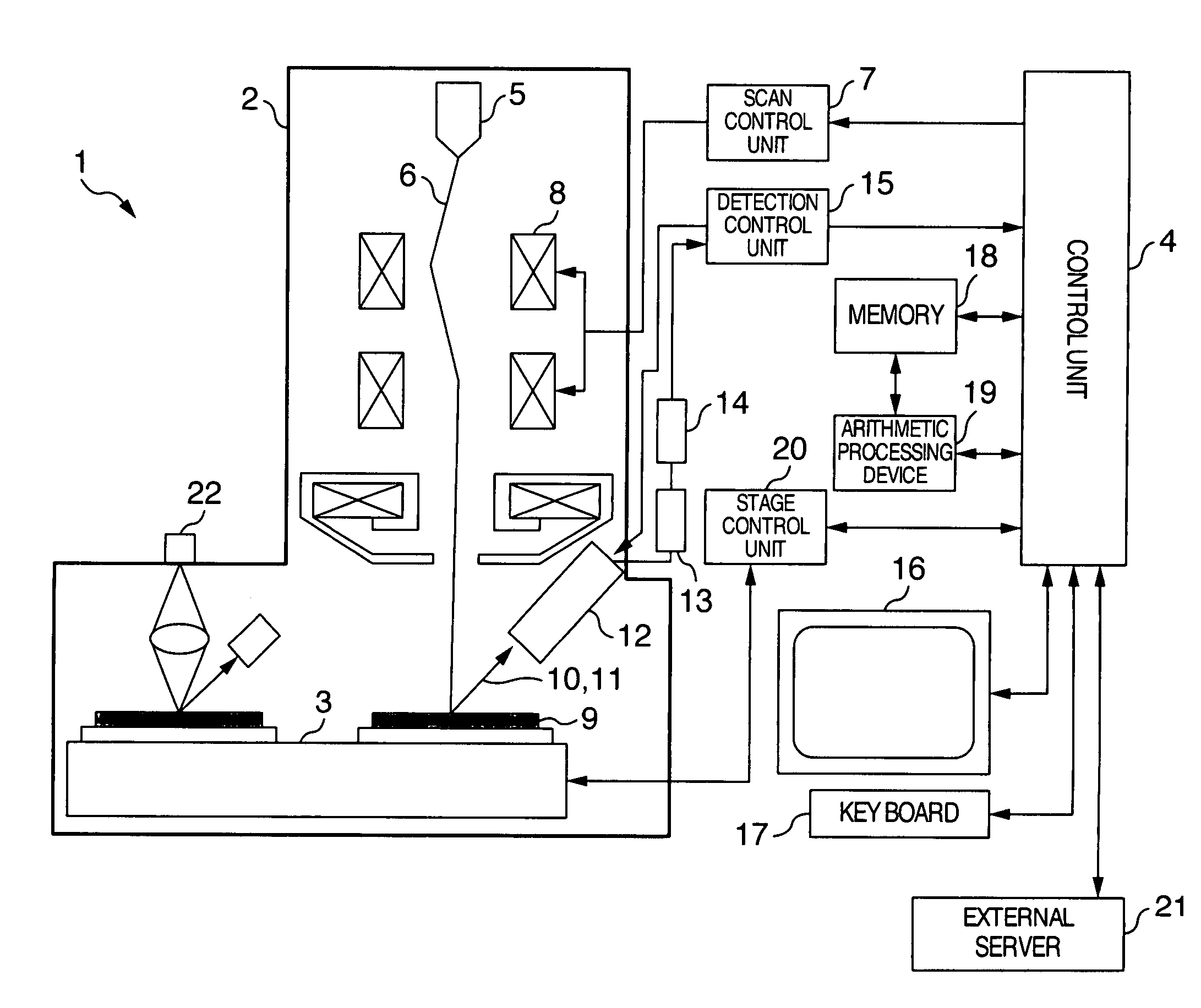
[0055] Referring to FIG. 1, there is shown in block diagram form a configuration of a semiconductor device inspection apparatus used in this invention. An electron beam 6 of high energy, which is emitted from an electron source 5, is deflected by a scanning coil 8 under the control of a scan control unit 7 and is then raster-scanned on a wafer 9. The scanning range of the electron beam 6 on the wafer 9 is determined by appropriately setting an output of the scan contr...
embodiment 2
[0067] In this embodiment, there will be explained one example of a taper angle inspection method of a pattern such as a gate electrode or the like. In this invention, the semiconductor device inspection apparatus having the configuration shown in FIG. 1 is usable. Here, the taper angle refers to an angle 33 defined by a substrate 25 and a sidewall 48 of the pattern such as a gate electrode in a cross-section of the pattern shown in FIG. 9C, which is an important parameter that determines the device characteristics.
[0068] When emitting a high-energy electron beam 35 onto the pattern having the taper angle 33 as shown in FIG. 9C, secondary electrons 10 and backscattered electrons 11 are generated from the substrate surface, resulting in a large number of secondary electrons 10 and backscatter electrons 11 being generated by the edge effect from sidewalls 48 of the pattern. In case the taper angle is 90° or greater, a large number of secondary electrons 36 and backscatter electrons 3...
embodiment 3
[0080] In this embodiment, there will be explained another example of the taper angle inspection method of a pattern such as a gate electrode or else. In this invention, the semiconductor device inspection apparatus with the arrangement shown in FIG. 1 can be used. Alternatively as shown in FIG. 20, a scanning semiconductor device inspection apparatus with a low-acceleration electron beam 64 and a high-acceleration electron beam 6 being as incident electron beams is usable. The high-acceleration electron beam 6 that is emitted from an electron source 5 is deflected by a scanning coil 8 under the control of a scan control unit 7 and is then raster-scanned on a wafer 9. Secondary electrons 10 and backscattered electrons 11 which are generated from a surface of the wafer 9 due to the scanning of the electron beam 6 are detected by a detector 12 and then amplified by an amplifier unit 13. An amplified secondary electron signal is displayed as a scan image on a monitor 16.
[0081] On the ...
PUM
 Abstract
Description
Claims
Application Information