Apparatus and plasma ashing process for increasing photoresist removal rate

a technology of ashing process and plasma, which is applied in the field of plasma ashing process, can solve the problems of limiting the overall chip speed, increasing the dielectric constant, and using gas sources that have proven detrimental to substrates containing low k dielectrics, and achieve the effect of reducing the temperature of the upper baffle pla

Inactive Publication Date: 2006-03-02
LAM RES CORP
View PDF15 Cites 173 Cited by
  • Summary
  • Abstract
  • Description
  • Claims
  • Application Information

AI Technical Summary

Benefits of technology

[0012] Disclosed herein are plasma ashing processes for removing photoresist, post etch residues and volatile byproducts from a substrate. In one embodiment, the plasma ashing process for removing photoresist material and post etch residues from a substrate comprising carbon, hydrogen, or a combination of carbon and hydrogen, wherein the substrate comprises a low k dielectric material comprises forming a p...

Problems solved by technology

As integrated devices become smaller, the RC-delay time of signal propagation along interconnects becomes one of the dominant factors limiting overall chip speed.
However, the wet chemical treatment can cause further degradation of the low k dielectric, loss of material, and can also cause an increase in the dielectric constant.
Although gas mixtures comprising these sources efficiently ash photoresist from the substrate, the use of these gas sources has proven detrimental to substrates containing low k dielectrics.
The increases in dielectric constant affects, among others things, interconnect capacitance, which directly impacts device performance.
Moreover, the use of oxygen-containing plasmas is generally less preferred for advanced device fabrication employing copper metal layers, since copper metal is readily oxidized.
An issue with low k dielectrics is ...

Method used


Image

  • Apparatus and plasma ashing process for increasing photoresist removal rate
  • Apparatus and plasma ashing process for increasing photoresist removal rate
  • Apparatus and plasma ashing process for increasing photoresist removal rate

Examples


example 2

[0063] In this example, a dual baffle plate assembly having an upper and lower plate spaced apart by about 0.5 inch was employed, where the upper quartz baffle plate was configured with the cooling gas conduit in the manner shown in FIG. 7. As previously discussed, the cooling gas conduit serves to both cool the upper baffle plate in the baffle plate assembly and provide a counter-flow to the plasma impinging on the upper baffle plate from above to prevent excessive heating. Helium gas was used to cool the upper baffle and was introduced at flows ranging from 0 to 440 sccm.

[0064] Wafers were coated with about 8,200 angstroms of Shipley UV-6 photoresist, baked, and the thickness measured. The coated wafers were then processed in the Axcelis Technologies asher as in Example 1. Flow rates were 10,000 sccm of 4% hydrogen in helium and 100 μL / min (microliters per minute) of oxygen. The runs differed only in the amount of counter-flow cooling helium supplied to the baffle plate. The thic...

example 3

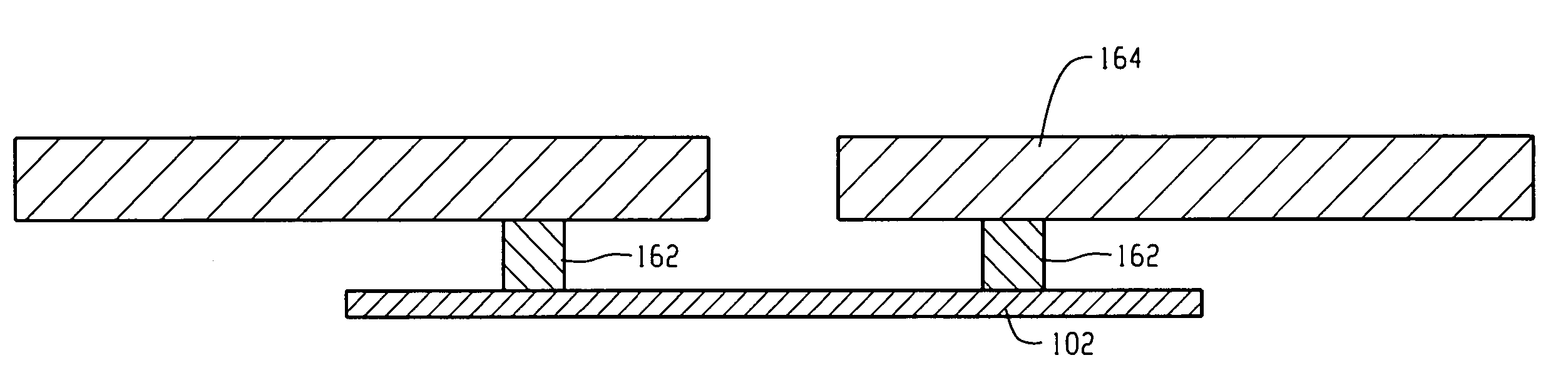
[0065] In this example, a comparison of two baffle plate designs were examined in the ES3Lk plasma asher commercially available from Axcelis Technologies, Inc. The plasma asher included a dual baffle plate assembly having an upper and lower plate separated by about 0.5 inch. In one comparative configuration, the upper baffle plate was constructed of quartz and was supported by 3 quartz legs resting on the lower baffle plate. The second configuration employed the use of a thermally conductive material. In this configuration as shown in FIG. 8, the upper baffle plate is formed of an aluminum plate suspended 0.5 inches from the lower baffle plate. Suspension is achieved by the use of mounting hardware formed of thermally conductive aluminum standoffs and appropriate connecting bolts to fixedly attach the upper baffle plate to the water-cooled lid of the plasma asher.

[0066] Wafers were coated with about 8,200 angstroms of Shipley UV-6 photoresist, baked and the thickness measured. The ...


PUM


Abstract

A plasma ashing process for removing photoresist material and post etch residues from a substrate comprising carbon, hydrogen, or a combination of carbon and hydrogen, wherein the substrate comprises a low k dielectric layer, the process comprising forming a plasma from an essentially oxygen free and nitrogen free gas mixture; introducing the plasma into a process chamber, wherein the process chamber comprises a baffle plate assembly in fluid communication with the plasma; flowing the plasma through the baffle plate assembly and removing photoresist material, post etch residues, and volatile byproducts from the substrate; periodically cleaning the process chamber by introducing an oxygen plasma into the process chamber; and cooling the baffle plate assembly by flowing a cooling gas over the baffle plate assembly. A process chamber adapted for receiving downstream plasma, the process chamber comprising an upper baffle plate comprising at least one thermally conductive standoff in thermal communication with a wall of the process chamber; and a lower baffle plate spaced apart from the upper baffle plate.

Description

CROSS REFERENCE TO RELATED APPLICATIONS [0001] The present application relates to and claims priority to U.S. Provisional Application No. 60 / 606,360, filed on Sep. 1, 2004, incorporated herein by reference in its entirety.BACKGROUND [0002] The present disclosure relates to semiconductor manufacturing, and more particularly, to plasma ashing processes for removing photoresist and post etch residues from a substrate. [0003] Recently, much attention has been focused on developing low k dielectric thin films for use in the next generation of microelectronics. As integrated devices become smaller, the RC-delay time of signal propagation along interconnects becomes one of the dominant factors limiting overall chip speed. With the advent of copper technology, R (resistance) has been pushed to its practical lowest limit. As such, attention is focused on reducing C (capacitance) in order to increase overall chip speed. One way of accomplishing this task is to reduce the dielectric constant (...

Claims


Application Information

Patent Timeline
IPC IPC(8): H01L21/4763
CPCG03F7/427H01J37/32192H01J37/32449H01L21/76814H01J2237/3342H01L21/0206H01L21/31138H01J37/32522H01L21/3065H01L21/02
Inventor BECKNELL, ALAN F.HAMMAR, PHILIPFERRIS, DAVID
Owner LAM RES CORP
Why Eureka
Try Eureka