

Integrated antenna type circuit apparatus
a technology of integrated antenna and circuit apparatus, which is applied in the direction of electrical apparatus construction details, semiconductor/solid-state device details, and printed electric component incorporation, etc., can solve the problems of difficult integration of semiconductor circuits to be used inside, difficult to sophisticate antenna performance, and difficult to integrate semiconductor chips and chip parts with other semiconductor chips and chip parts, etc., to reduce the area of antenna conductors, improve emission efficiency, and suppress the effect of increasing the packaging area
- Summary
- Abstract
- Description
- Claims
- Application Information
AI Technical Summary
Benefits of technology
Problems solved by technology
Method used
Image

Examples
first embodiment
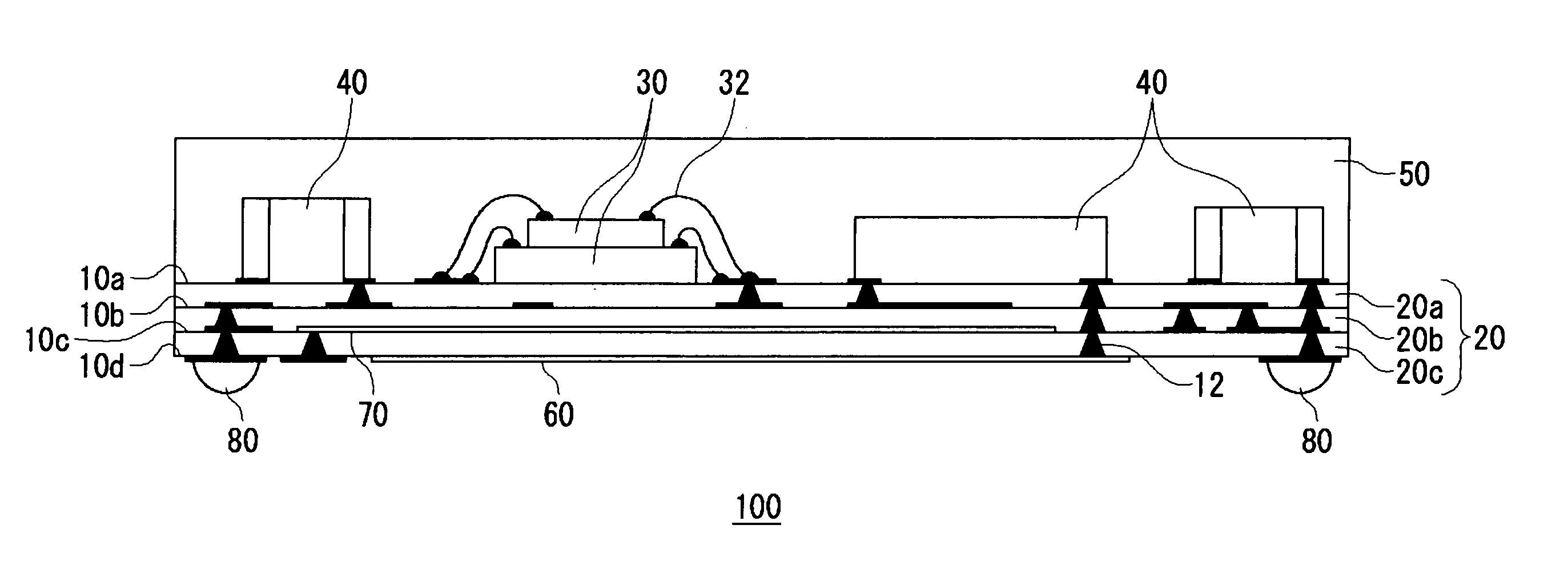
[0045]FIG. 1 is a sectional view of an integrated antenna type circuit apparatus 100 according to a first embodiment. The integrated antenna type circuit apparatus 100 includes an insulating base 20, semiconductor circuit devices 30, chip parts 40, a molding resin 50, an antenna conductor 60, a ground conductor 70, and external lead electrodes 80. For the sake of convenience, in FIG. 1, the side on which the chip parts 40 are mounted shall be referred to as being upward, and the side on which the external lead electrodes 80 are formed being downward.
[0046] An example of the semiconductor circuit devices 30 is an IC chip in which transistors, diodes, and passive elements are integrated. The semiconductor circuit devices 30 are formed on a semiconductor substrate made of silicon, silicon germanium, gallium arsenide, or the like. By such means as a silver paste, the semiconductor circuit devices 30 are die bonded to the insulating base 20 for physical connection. Electrode pads of the...
second embodiment
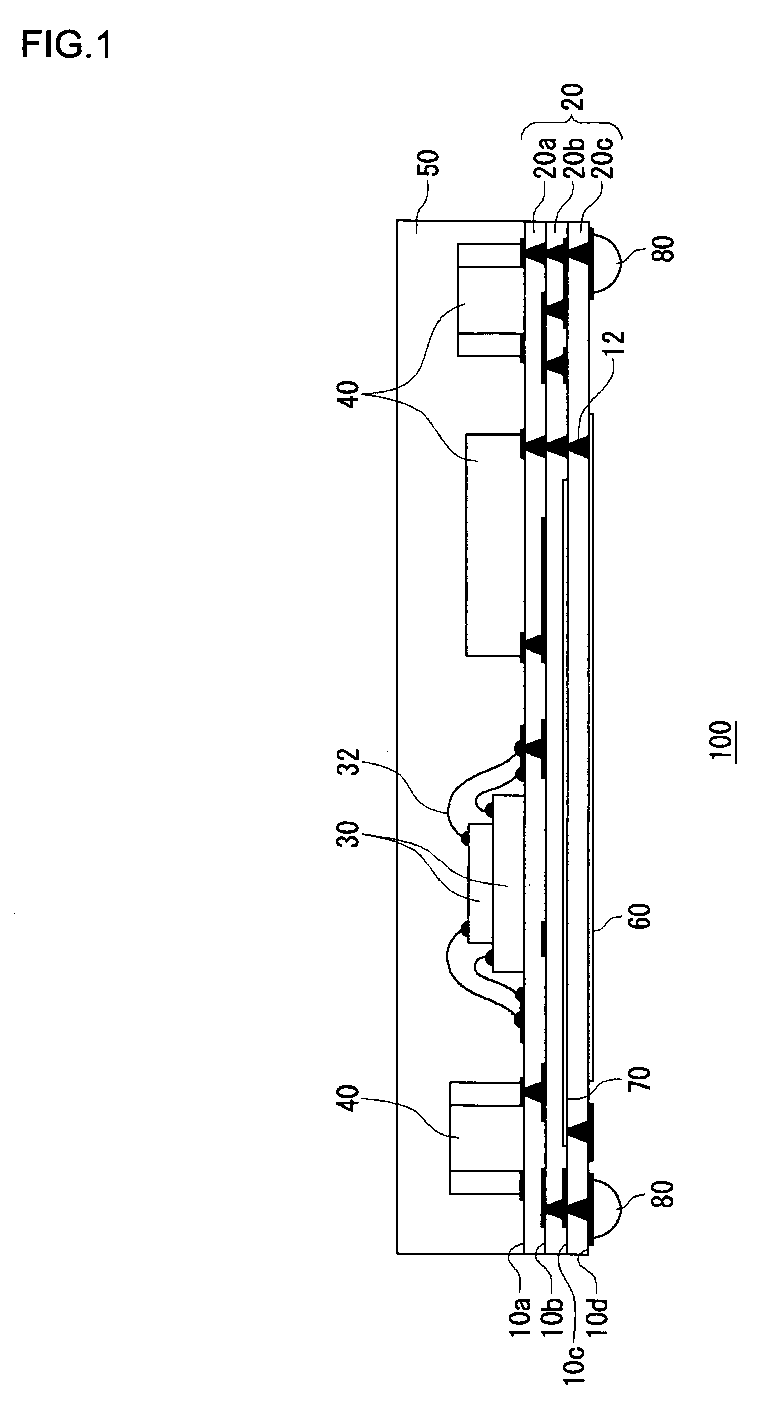
[0074] In the first embodiment, the components of the radio frequency circuit, i.e., the semiconductor circuit devices 30 and the plurality of chip parts 40 are formed on the insulating base 20 and sealed by the molding resin 50 so as to be embedded in the insulator layer.
[0075] In the integrated antenna type circuit apparatuses 100 according to second and subsequent embodiments to be described below, the semiconductor circuit devices 30 and the plurality of chip parts 40 are embedded in the insulating base 20. In the following embodiments, description of the same configuration as in the first embodiment will be omitted as appropriate.
[0076]FIG. 2 is a sectional view showing the configuration of the integrated antenna type circuit apparatus 100 according to the second embodiment. For ease of explanation, the side on which the chip components 40 are mounted shall be referred to as being upward, and the side on which the external lead electrodes 80 are formed being downward.
[0077] ...
third embodiment
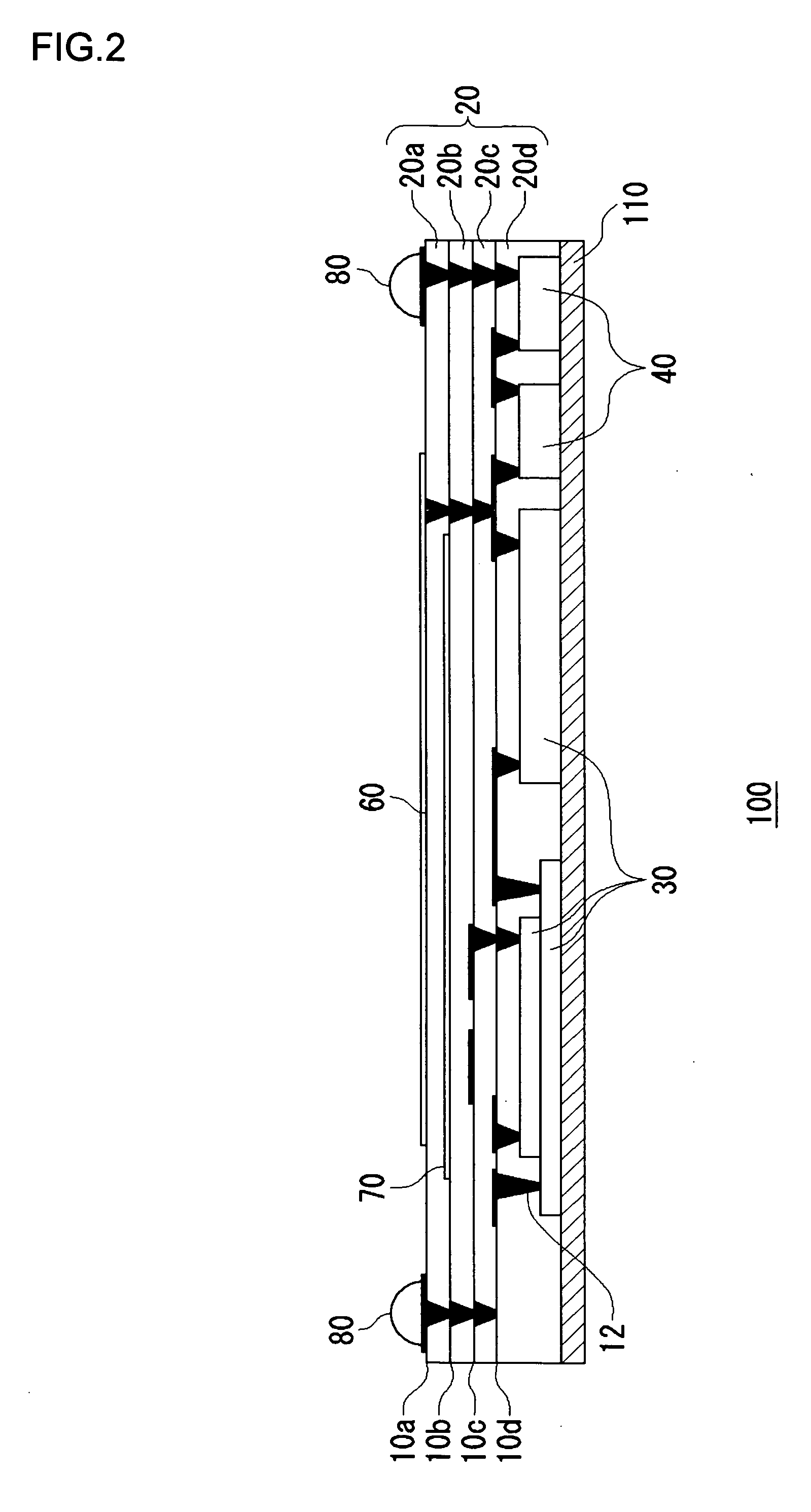
[0089]FIG. 3 is a sectional view showing the configuration of the integrated antenna type circuit apparatus 100 according to a third embodiment. In the integrated antenna type circuit apparatus 100 shown in FIG. 2, the external lead electrodes 80 and the antenna conductor 60 are formed on the same side. In the present embodiment, the antenna conductor 60 is arranged on a side different from the external lead electrodes 80 are.
[0090] In other words, the present embodiment differs from the second embodiment in that the base 110 is also provided with via plugs 12 so as to establish connection between the external lead electrodes 80 and the wiring conductors. In other respects, the structure is the same as in the second embodiment.
[0091] In addition to the effects of the second embodiment described above, the present embodiment provides the following effects.
[0092] Since the antenna conductor 60 and the external lead electrodes 80 are formed on the opposite sides, the antenna falls o...
PUM
 Abstract
Description
Claims
Application Information