Transfer mask blank, transfer mask, and transfer method using the transfer mask

a transfer mask and mask technology, applied in the field of transfer masks, can solve the problems of deteriorating the position accuracy of patterns, affecting the quality of microlithography, and the inability of photomask writers to write high-accuracy patterns to substrates without photomask shapes, etc., to achieve the effect of easily transferring an accurate and fine pattern, and effective and accurate manufacturing

Inactive Publication Date: 2006-03-30
DAI NIPPON PRINTING CO LTD
View PDF6 Cites 2 Cited by
  • Summary
  • Abstract
  • Description
  • Claims
  • Application Information

AI Technical Summary

Benefits of technology

[0051] The present invention is made in order to solve the above described problems. It is an object of the present invention to provide a lithography mask blank which allows a charged-particle beam lithography mask such as electron beams, an X-ray lithography mask, an extreme ultraviolet beam lithography mask to be effectively manufactured by using an existing writer such as an electron beam writer for photomasks and with improved processing accuracy of mask pattern, and to provide a lithography mask manufactured from such a lithography mask blank. It is another object of the present invention to provide a lithography using such a lithography mask.
[0061] In the present invention, since the shape of the substrate is a substantially rectangular parallelepiped and the pattern region at substantially the center and the peripheral region of the upper surface of the substrate are in one plane, a charged-particle beam lithography mask, an X-ray lithography mask, or an extreme ultraviolet beam lithography mask having a fine pattern can be effectively and accurately manufactured by using, for example, an existing electron beam writer for photomasks. Therefore, it is possible to easily transfer an accurate and fine pattern from such a lithography mask to a resist.

Problems solved by technology

If a large number of semiconductor integrated circuits are disposed, the number of semiconductor integrated circuits to be transferred at once is increased so as to increase the productivity, while a problem of deteriorating the positional accuracy of pattern is caused in case of a mask having a large area membrane.
6(a)-6(b) have a disadvantage that a photomask manufacturing apparatus is hardly employed in processes for manufacturing a mask, such as an electron beam writing process, a dry-etching process, a particle-detecting process, a defect-detecting process, and a pattern-size-measuring process by a scanning electron microscope.
Since the pattern on the photomask is written by an electron beam writer, the writer for photomasks is specialized for photomasks so that the writer for photomasks can not write high-accuracy pattern to a substrate not having a photomask shape.
However, if one attempts to use the electron beam writer for photomasks to the blank of this example, one will find a problem that it is hard to keep the surface to be patterned (hereinafter, referred to as a pattern region surface) in a focusing range of electron beams.
If the pattern region surface (the upper surface coated with the electron beam resist) of the photomask blank 50 shifts largely from the electron beam focusing surface, it causes deterioration of a resist pattern image.
If the focusing surface of electron beams is apart from the reference surface by 0.3 mm or more, a problem of not obtaining high positional accuracy is caused.
Accordingly, there may be a problem that the height of the pattern region surface shifts largely from the focusing area of electron beams due to the inclination of the upper surface of the substrate 41.
Consequently, there is a problem that it is not possible to accurately write a mask pattern on the pattern region at the center of the blank.

Method used


Image

  • Transfer mask blank, transfer mask, and transfer method using the transfer mask
  • Transfer mask blank, transfer mask, and transfer method using the transfer mask
  • Transfer mask blank, transfer mask, and transfer method using the transfer mask

Examples


Embodiment Construction

[0071] Hereinafter, a lithography mask of the present invention and a lithography mask blank for manufacturing the same will be described with reference to embodiments.

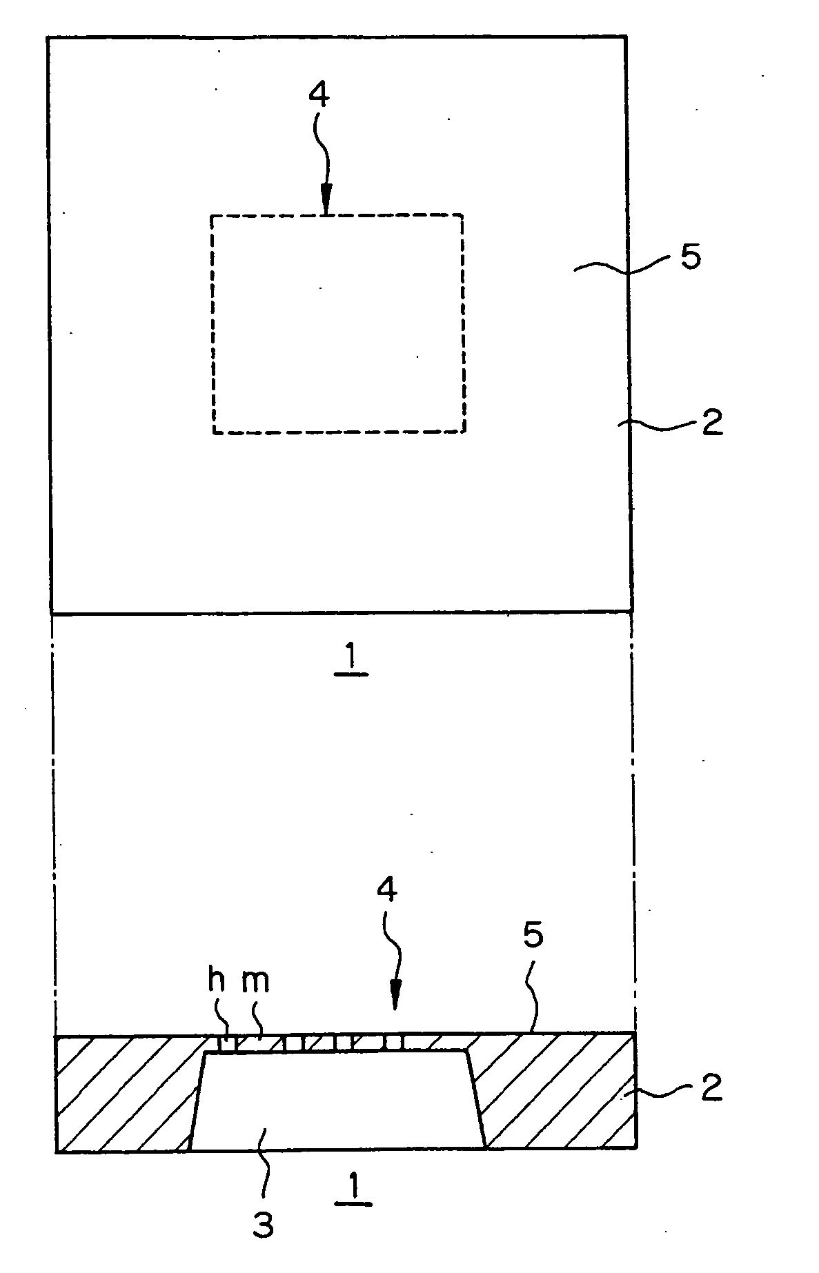
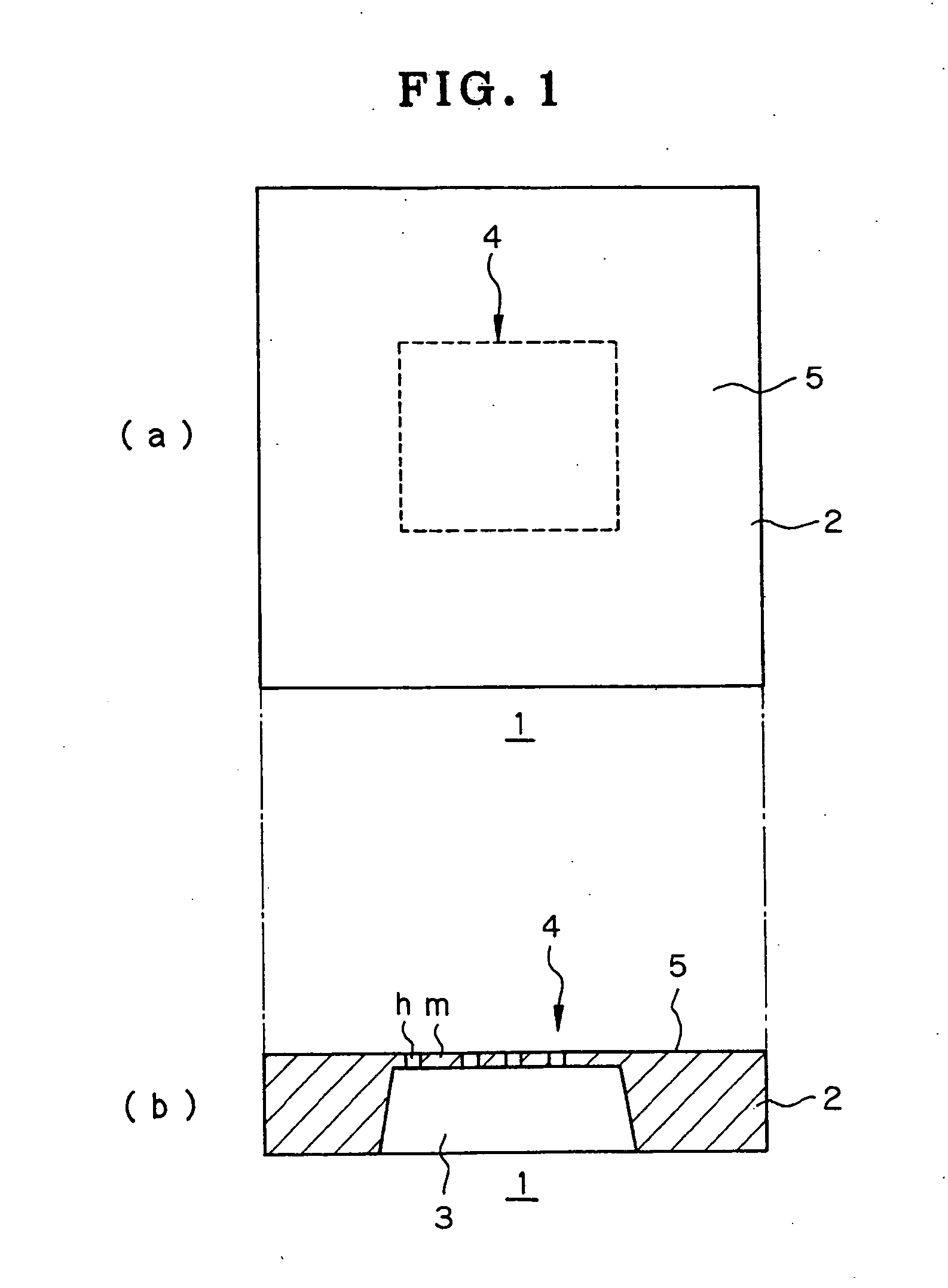
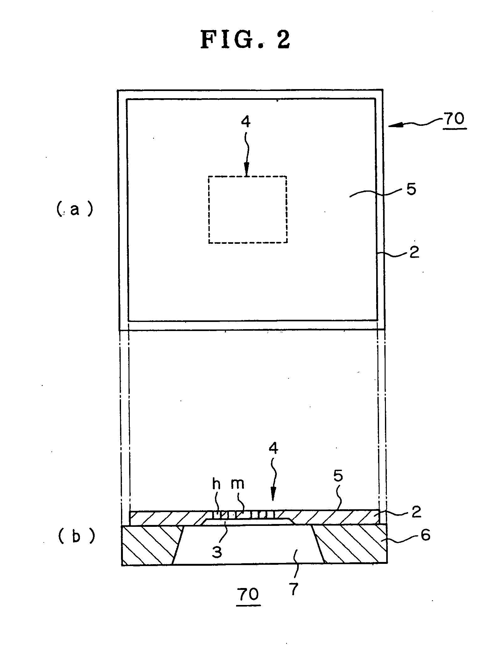
[0072] FIGS. 1(a) and 1(b) are a plan view (a) and a sectional view (b) of an embodiment of a stencil-type lithography mask according to the present invention. The mask 1 comprises a substrate 2 which is provided with a pattern region 4 over an opening 3 formed in the center thereof. The pattern region 4 lies on a self-supporting membrane “m” in which patterned holes “h” are formed. A peripheral region 5, which is a part of the upper surface of the substrate 2, is arranged around the outer periphery of the pattern region 4. The shape of the mask 1 is a substantially rectangular parallelepiped which is formed as a unit such that the pattern region 4 and the peripheral region 5 are in one plane. The stencil-type lithography mask 1 is used as a lithography mask for X-ray or charged-particle beams.

[0073] A lithography m...


PUM

PropertyMeasurementUnit
wavelengthsaaaaaaaaaa

Abstract

It is an object of the present invention to effectively manufacture a charged-particle beam lithography mask, an X-ray lithography mask, or an extreme ultraviolet beam lithography mask by using, for example, an existing writer such as an electron beam writer for photomasks, while achieving improvement in processing accuracy of a mask pattern. A lithography mask (1) comprises a substrate (2) which has a lower surface provided substantially at the center thereof with an opening (3) and a self-supporting membrane (m) having a pattern region (4) substantially at the center of an upper surface of the substrate (2) corresponding to the opening (3). The self-supporting membrane (m) is provided with through-holes (h) of a mask pattern in it or an absorber or scatterer of a mask pattern on it, and the pattern region (4) and a peripheral region around the pattern region (5) are in one plane.

Description

TECHNICAL FIELD [0001] The present invention relates to a lithography mask and a lithography mask blank to be used in the lithography process for manufacturing semiconductor integrated circuit devices and a lithography using the lithography mask. More particularly, the present invention relates to a lithography mask and a lithography mask blank for proximity electron-beam projection lithography, a lithography using the lithography mask and further relates to a lithography mask blank for a lithography mask for other lithographies using charged-particle beams, X-ray, or extreme ultraviolet beam, and a lithography using the lithography mask. BACKGROUND ART [0002] In the lithography process for manufacturing semiconductor integrated circuit devices, a pattern transfer by an optical reduction projection exposure with a photomask (sometimes, called reticle) is generally conducted. Electromagnetic waves used for the exposure are i-line (having a wavelength of 365 nm), KrF excimer laser lig...

Claims


Application Information

Patent Timeline
Patent Type & Authority Applications(United States)
IPC IPC(8): G03F1/00G03F1/20G03F1/22G03F1/24G03F1/68G03F7/20H01L21/027
CPCG03F1/20G03F1/22G03F7/2063G03F1/78G03F1/24
Inventor SANO, HISATAKEHOGA, MORIHISAIIMURA, YUKIOARITSUKA, YUKIKURIHARA, MASAAKINOZUE, HIROSHIYOSHIDA, AKIRA
Owner DAI NIPPON PRINTING CO LTD
Why Eureka
Try Eureka