Wafer polishing method and apparatus

a polishing method and polishing technology, applied in the direction of grinding machine components, manufacturing tools, lapping machines, etc., can solve the problems of limited mechanical improvements, limited improvement, and limited film thickness and uniformity, and achieve the effect of preventing the peripheral sag of the wafer and high flatness level

Active Publication Date: 2006-03-30
SHIN-ETSU HANDOTAI CO LTD
View PDF11 Cites 8 Cited by
  • Summary
  • Abstract
  • Description
  • Claims
  • Application Information

AI Technical Summary

Benefits of technology

[0018] The present invention has been made in light of the problems of the conventional technique and it is an object of the present invention to provide a wafer polishing method and

Problems solved by technology

However, the thus adhered SOI wafer 50 is subjected to mechanical processing such as grinding or polishing into a thin film, and hence the obtained SOI layer 52 have limitations in its film thickness and uniformity thereof.
However, attempts have been made to process a wafer to a high flatness level by contriving a mechanism of a polishing head or the like, but the

Method used


Image

  • Wafer polishing method and apparatus
  • Wafer polishing method and apparatus
  • Wafer polishing method and apparatus

Examples


example 1

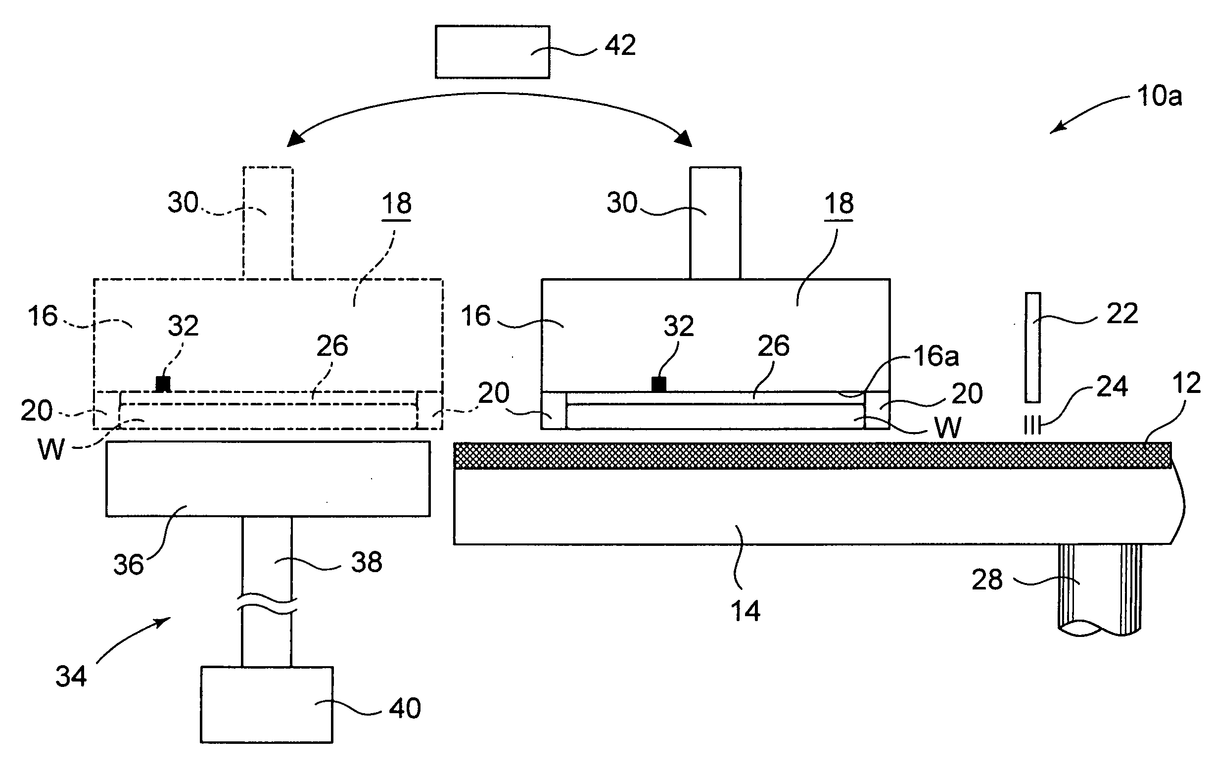
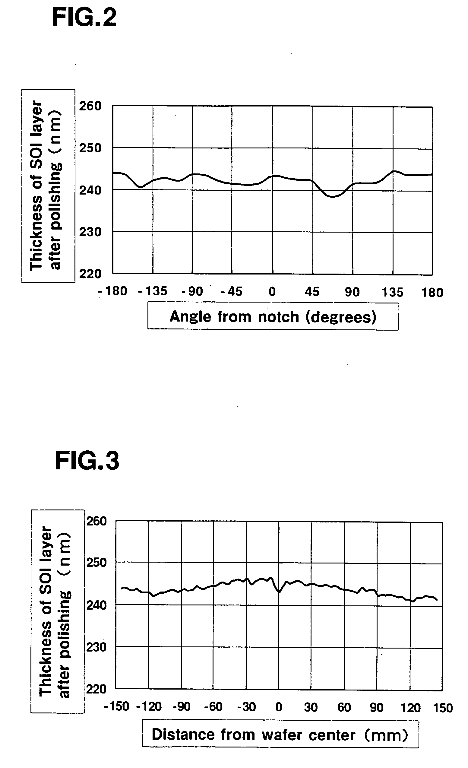
[0055] Plural wafers manufactured by means of an ion implantation separation method as SOI wafers serving as polishing objects were provided to be ready for use. The wafers as starting raw materials each had parameters, such as a diameter of an SOI wafer of 300 mm, a thickness of a support substrate of about 775 nm, a thickness of an oxide film layer is about 145 nm and a thickness of an SOI layer of about 340 nm, and description will be given of a case where polishing was carried out with a total polishing stock removal of about 90 nm as an example.

[0056] There was employed as a polishing apparatus F-REX300 manufactured by Ebara Corporation to polish the SOI wafers. A suede type polishing cloth, Ciegal 7355fm (a lattice groove of 20 mm square) manufactured by Toray Coatex Co., Ltd. was used as a polishing cloth, and G33900RS manufactured by Fujimi Incorporated was employed as a polishing agent. A polishing pressure was 240 g / cm2.

[0057] Since a target polishing stock removal (a to...


PUM

PropertyMeasurementUnit
Angleaaaaaaaaaa

Abstract

The present invention provides a wafer polishing method and a polishing apparatus which are capable of preventing peripheral sags of a wafer due to polishing and then manufacturing the wafer, especially an SOI wafer at a high flatness level. There is provided a wafer polishing method using a polishing apparatus which comprises a rotatable table having a polishing cloth adhered thereon and a polishing head equipped with a wafer holding plate opposing to the table and in which the back surface of the wafer is held by a holding surface of the wafer holding plate and the front surface of the wafer is pressed to and polished by the polishing pad, comprising a polishing step of polishing the front surface of the wafer to a predetermined total polishing stock removal without changing the polishing apparatus, wherein the polishing step is divided into plural sub-steps and a holding position of the wafer in a subsequent sub-step is different from a holding position of the wafer in a previous sub-step.

Description

TECHNICAL FIELD [0001] The present invention relates to a wafer polishing method and a polishing apparatus which are capable of preventing peripheral sags of a wafer due to polishing and then manufacturing the wafer, especially an SOI (Silicon on Insulator) wafer at a high flatness level. BACKGROUND ART [0002] In recent years, in order to improve a yield in a device process, a requirement for a high flatness level of a semiconductor wafer such as a silicon wafer has been more and more enhanced. A manufacturing method for a mirror polished wafer with such a high flatness level has been generally constituted of: a single crystal growing process producing a single crystal ingot using a Czochralski (CZ) method, a Floating Zone (FZ) method or the like; and a wafer manufacturing (processing) process slicing the single crystal ingot into sliced wafers to process at least one main surface of each of the sliced wafers into a mirror polished surface. With thus manufactured mirror-polished waf...

Claims


Application Information

Patent Timeline
IPC IPC(8): B24B49/00B24B1/00B24B37/04B24B37/30B24B37/32H01L21/304H01L21/306H01L21/762
CPCB24B37/042B24B37/30H01L21/76254H01L21/02024B24B37/345
Inventor TSUCHIYA, TOSHIHIRO
Owner SHIN-ETSU HANDOTAI CO LTD
Why Eureka
Try Eureka